Star News


Reverse collector current of a bipolar transistor. Bipolar transistor, transistor cascade calculation
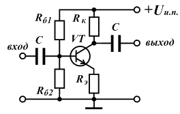
The circuit for switching on a bipolar transistor with a common emitter is shown in Figure 5.15:
The characteristics of the transistor in this mode will be different from those in common base mode. In a transistor connected according to a common emitter circuit, there is an amplification not only in voltage, but also in current. The input parameters for a circuit with a common emitter will be the base current I b, and the collector voltage U k, and the output characteristics will be the collector current I k and the voltage at the emitter U e.
Earlier, when analyzing a bipolar transistor in a common base circuit, the relationship between the collector current and the emitter current was obtained in the following form:
In a common emitter circuit (according to Kirchhoff's first law).
after rearranging the factors, we get:

Rice. 5.15. Switching circuit for a transistor with a common emitter
The coefficient α / (1-α) in front of the factor I b shows how the collector current I k changes with a single change in the base current I b. It is called the current gain of a bipolar transistor in a common emitter circuit. We denote this coefficient by β.
(5.31)Since the value of the transfer coefficient α is close to unity (α > 1). With the values of the transfer coefficient α = 0.98÷0.99, the gain will lie in the range β = 50÷100.
Taking into account (5.31), as well as I k0 * = I k0 / (1-α), expression (5.30) can be rewritten as:
where I k0 * \u003d (1 + β) I k0 is the thermal current of a single p-n junction, which is much greater than the thermal current of the collector I k0, and the value of r k is defined as r k * = r k / (1 + β).
Differentiating equation (5.32) with respect to the base current I b, we obtain β = ΔI to /ΔI b. It follows that the gain β shows how many times the collector current I k changes when the base current I b changes.
To characterize the value of β as a function of the parameters of a bipolar transistor, we recall that the emitter current transfer coefficient is defined as α = γ κ, where . Consequently, ![]() . For the value of β, the following value was obtained: β = α/(1-α). Since W/L
. For the value of β, the following value was obtained: β = α/(1-α). Since W/L 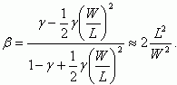 (5.33)
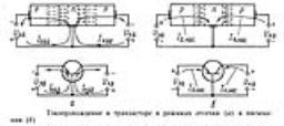
Figure 5.16a shows the current-voltage characteristics of a bipolar transistor connected according to a circuit with a common emitter with a base current as a parameter of the curves. Comparing these characteristics with similar characteristics for a bipolar transistor in a common base circuit, it can be seen that they are qualitatively similar.
Let us analyze why small changes in the base current I b cause significant changes in the collector current I k. The value of the coefficient β, which is significantly greater than one, means that the transfer coefficient α is close to one. In this case, the collector current is close to the emitter current, and the base current (recombination by physical nature) is much smaller than both the collector and emitter currents. When the value of the coefficient α = 0.99 out of 100 holes injected through the emitter junction, 99 are extracted through the collector junction, and only one will recombine with the electrons in the base and contribute to the base current.
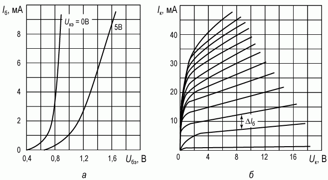
Rice. 5.16. Volt-ampere characteristics of the bipolar transistor KT215V, connected according to the scheme with a common emitter:
a) input characteristics; b) output characteristics
Doubling the base current (two holes should recombine) will cause twice as much injection through the emitter junction (200 holes should be injected) and, accordingly, extraction through the collector junction (198 holes should be extracted). Thus, a small change in the base current, for example from 5 to 10 µA, causes large changes in the collector current, respectively from 500 µA to 1000 µA.
TRANSISTOR- a semiconductor device for amplifying, generating and converting electrical oscillations, made on the basis of a single-crystal semiconductor ( Si- silicon, or Ge- germanium) containing at least three regions with different - electronic ( n) and hole ( p) - conductivity. Invented in 1948 by the Americans W. Shockley, W. Brattain, and J. Bardeen. According to the physical structure and current control mechanism, bipolar transistors (more often called simply transistors) and unipolar transistors (more often called field-effect transistors) are distinguished. In the former, containing two or more electron-hole transitions, both electrons and holes serve as charge carriers, and in the latter, either electrons or holes. The term "transistor" is often used to refer to portable radio broadcast receivers based on semiconductor devices.
The current in the output circuit is controlled by changing the input voltage or current. A small change in input values can lead to a much larger change in output voltage and current. This amplifying property of transistors is used in analog technology (analog TV, radio, communications, etc.).
In this article, we will look at a bipolar transistor
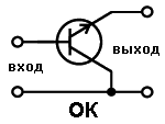
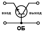
The bipolar transistor can be n-p-n and p-n-p conductivity. Without looking into the insides of the transistor, one can note the difference in conductivity only in the polarity of the connection in practical circuits of power supplies, capacitors, diodes, which are part of these circuits. The figure on the right graphically shows n-p-n and p-n-p transistors.
The transistor has three terminals. If we consider the transistor as a four-pole, then it should have two input and two output terminals. Therefore, some of the conclusions must be common, both for the input and for the output circuit.
Transistor switching circuits
 Switching circuit for a transistor with a common emitter– designed to amplify the amplitude of the input signal in terms of voltage and current. In this case, the input signal, amplified by the transistor, is inverted. In other words, the phase of the output signal is rotated 180 degrees. This circuit is the main one for amplifying signals of different amplitudes and shapes. The input resistance of a transistor stage with OE is from hundreds of ohms to units of kilo-ohms, and the output resistance is from units to tens of kilo-ohms.
 Scheme for switching on a transistor with a common collector– designed to amplify the amplitude of the input signal by current. Voltage amplification does not occur in such a circuit. More correctly, the voltage gain is even less than unity. The input signal is not inverted by the transistor.
The input resistance of a transistor cascade with OK is from tens to hundreds of kilo-ohms, and the output resistance is within hundreds of ohms - units of kilo-ohms. Due to the fact that, as a rule, a load resistor is located in the emitter circuit, the circuit has a large input resistance. In addition, due to the amplification of the input current, it has a high load capacity. These properties of the common collector circuit are used to match the transistor stages - as a "buffer stage". Since, the input signal, without amplifying in amplitude, "repeats" at the output, the circuit for switching on a transistor with a common collector is also called emitter follower.
 There is more Scheme of switching on a transistor with a common base. This inclusion scheme exists in theory, but in practice it is very difficult to implement. Such a switching circuit is used in high-frequency technology. Its peculiarity is that it has a low input impedance, and it is difficult to coordinate such a cascade at the input. My experience in electronics is not small, but speaking of this transistor switching circuit, I'm sorry, I don't know anything! I used it a couple of times as a "foreign" scheme, but I never understood it. Let me explain: according to all physical laws, the transistor is controlled by its base, or rather by the current flowing along the base-emitter path. Using the input terminal of the transistor - the base at the output - is not possible. In fact, the base of the transistor is "planted" through a capacitor at a high frequency on the case, but it is not used at the output. And galvanically, through a high-resistance resistor, the base is connected to the output of the cascade (a bias is applied). But you can apply an offset, in fact, from anywhere, even from an additional source. Anyway, a signal of any shape that enters the base is quenched through the same capacitor. In order for such a cascade to work, the input output - the emitter is "planted" on the case through a low-resistance resistor, hence the low input resistance. In general, the switching circuit of a transistor with a common base is a topic for theorists and experimenters. In practice, it is extremely rare. In my practice in designing circuits, I have never encountered the need to use a common-base transistor switching circuit. This is explained by the properties of this switching circuit: input resistance - from units to tens of ohms, and output resistance - from hundreds of kilo-ohms to units of mega-ohms. Such specific parameters are a rare need.
A bipolar transistor can operate in switching and linear (amplifying) modes. The key mode is used in various control schemes, logic circuits, etc. In the key mode, the transistor can be in two operating states - open (saturated) and closed (locked) state. The linear (amplifying) mode is used in harmonic signal amplification circuits and requires the transistor to be kept in a "half" open, but not saturated state.
 To study the operation of a transistor, we will consider the switching circuit of a common emitter transistor as the most important switching circuit.
The scheme is shown in the figure. On the diagram VT- the transistor itself. Resistors R b1 and R b2- transistor bias circuit, which is an ordinary voltage divider. It is this circuit that ensures the transistor is shifted to the “working point” in the harmonic signal amplification mode without distortion. Resistor R to- load resistor of the transistor stage, designed to supply the collector of the transistor with an electric current of the power source and limit it in the "open" transistor mode. Resistor R e- feedback resistor, inherently increases the input impedance of the stage, while reducing the gain of the input signal. Capacitors C perform the function of galvanic isolation from the influence of external circuits.
To make it clearer to you how a bipolar transistor works, we will draw an analogy with a conventional voltage divider (see figure below). First, the resistor R2 we make the voltage divider controllable (variable). By changing the resistance of this resistor, from zero to "infinitely" of great importance, we can get at the output of such a divider a voltage from zero to the value supplied to its input. Now, imagine that the resistor R1 voltage divider is the collector resistor of the transistor stage, and the resistor R2 The voltage divider is the collector-emitter junction of the transistor. At the same time, by applying a control action in the form of an electric current to the base of the transistor, we change the resistance of the collector-emitter junction, thereby changing the parameters of the voltage divider. The difference from a variable resistor is that the transistor is driven by a low current. This is how a bipolar transistor works. The above is depicted in the figure below: 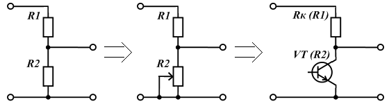
For the transistor to work in the signal amplification mode, without distorting the latter, it is necessary to provide this very operating mode. They talk about the displacement of the base of the transistor. Competent specialists amuse themselves with the rule: The transistor is controlled by current - this is an axiom. But the bias mode of the transistor is set by the base-emitter voltage, not by current - this is a reality. And for someone who does not take into account the bias voltage, no amplifier will work. Therefore, in the calculations, its value should be taken into account.
So, the operation of a bipolar transistor cascade in amplification mode occurs at a certain bias voltage at the base-emitter junction. For a silicon transistor, the bias voltage value lies in the range of 0.6 ... 0.7 volts, for germanium - 0.2 ... 0.3 volts. Knowing about this concept, you can not only calculate transistor stages, but also check the health of any transistor amplifier stage. It is enough to measure the bias voltage of the base-emitter of the transistor with a multimeter with a high internal resistance. If it does not correspond to 0.6 ... 0.7 volts for silicon, or 0.2 ... 0.3 volts for germanium, then look for a malfunction right here - either the transistor is faulty, or the bias or decoupling circuits of this transistor stage are faulty.
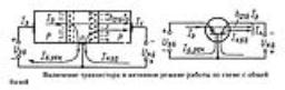
The above is shown on the graph - current-voltage characteristic (CVC). 
Most of the "specialists", looking at the presented CVC, will say: What kind of nonsense is drawn on the central graph? So the output characteristic of the transistor does not look like! It is shown on the right graph! I will answer, everything is correct there, but it started with electron vacuum tubes. Previously, the current-voltage characteristic of the lamp was considered to be the voltage drop across the anode resistor. Now, they continue to measure on the collector resistor, and on the graph they attribute letters indicating the voltage drop across the transistor, in which they are deeply mistaken. On the left graph I b - U be the input characteristic of the transistor is presented. On the central chart I to - U ke the output current-voltage characteristic of the transistor is presented. And on the right graph I R – U R the current-voltage graph of the load resistor is presented R to, which is usually given as the current-voltage characteristic of the transistor itself.
The graph has a linear section used for linear amplification of the input signal, limited by points BUT and FROM. Middle point - AT, is exactly the point at which it is necessary to contain a transistor operating in amplifying mode. This point corresponds to a certain bias voltage, which is usually taken in calculations: 0.66 volts for a silicon transistor, or 0.26 volts for a germanium transistor.
According to the current-voltage characteristic of the transistor, we see the following: in the absence or low bias voltage at the base-emitter junction of the transistor, the base current and collector current are absent. At this moment, the entire voltage of the power supply drops at the collector-emitter junction. With a further increase in the bias voltage of the base-emitter of the transistor, the transistor begins to open, the base current appears and the collector current increases with it. Upon reaching the "working area" at the point FROM, the transistor enters a linear mode that continues until the point BUT. In this case, the voltage drop at the collector-emitter junction decreases, and at the load resistor R to, on the contrary, increases. Dot AT- the operating point of the bias of the transistor, is such a point at which, as a rule, a voltage drop equal to exactly half the voltage of the power source is set at the collector-emitter junction of the transistor. Frequency response segment from a point FROM, to the point BUT called the displacement workspace. After the dot BUT, the base current and therefore the collector current increase sharply, the transistor opens completely - enters saturation. At this moment, at the collector-emitter junction, the voltage due to the structure drops n-p-n transitions, which is approximately equal to 0.2 ... 1 volt, depending on the type of transistor. All other voltage of the power supply drops on the load resistance of the transistor - resistor R to., which also limits the further increase in the collector current.
According to the lower "additional" figures, we see how the voltage at the output of the transistor changes depending on the signal applied to the input. The output voltage (collector voltage drop) of the transistor is out of phase (180 degrees) to the input signal.
Calculation of a transistor cascade with a common emitter (CE)
Before proceeding directly to the calculation of the transistor cascade, let's pay attention to the following requirements and conditions:
The calculation of the transistor cascade is carried out, as a rule, from the end (i.e. from the output);
To calculate the transistor stage, you need to determine the voltage drop at the collector-emitter junction of the transistor in rest mode (when there is no input signal). It is chosen so as to obtain the most undistorted signal. In a single-cycle transistor stage operating in "A" mode, this is usually half the voltage of the power supply;
Two currents run in the emitter circuit of the transistor - the collector current (along the collector-emitter path) and the base current (along the base-emitter path), but since the base current is small enough, it can be neglected and assumed that the collector current is equal to the emitter current;
A transistor is an amplifying element, so it is fair to say that its ability to amplify signals must be expressed by some value. The gain value is expressed by an indicator taken from the theory of quadripoles - the base current amplification factor in the switching circuit with a common emitter (OE) and it is denoted - h 21. Its value is given in reference books for specific types of transistors, and, usually, a plug is given in reference books (for example: 50 - 200). For calculations, one usually chooses minimum value(from the example we choose the value - 50);
Collector ( R to) and emitter ( R e) resistances affect the input and output resistances of the transistor stage. We can assume that the input impedance of the cascade R in \u003d R e * h 21, and the output is R out \u003d R to. If you do not care about the input resistance of the transistor stage, then you can do without a resistor at all R e;
Resistor ratings R to and R e limit the currents flowing through the transistor and the power dissipated by the transistor.
The order and example of calculating a transistor cascade with OE
Initial data:
Supply voltage U i.p.=12 V.
We select a transistor, for example: Transistor KT315G, for it:
Pmax=150 mW; Imax=150 mA; h 21>50.
Accept R to \u003d 10 * R e
Voltage b-e working take transistor points U bae= 0.66 V
Solution:
1. Let us determine the maximum static power that will be dissipated by the transistor at the moments of the passage of an alternating signal through the operating point B of the static mode of the transistor. It should be a value that is 20 percent less (a factor of 0.8) of the maximum power of the transistor indicated in the reference book.
Accept P ras.max \u003d 0.8 * P max\u003d 0.8 * 150 mW \u003d 120 mW
2. Determine the collector current in static mode (no signal):
I k0 \u003d P ras.max / U ke0 \u003d P ras.max / (U i.p. / 2)= 120mW/(12V/2) = 20mA.
3.
Considering that half of the supply voltage drops on the transistor in static mode (no signal), the second half of the supply voltage will drop across the resistors:
(R k + R e) \u003d (U i.p. / 2) / I k0\u003d (12V / 2) / 20mA \u003d 6V / 20mA \u003d 300 Ohms.
Given the existing range of resistor values, as well as the fact that we have chosen the ratio R to \u003d 10 * R e, we find the values of the resistors: R to= 270 Ohm; R e= 27 Ohm.
4. Find the voltage at the collector of the transistor without a signal. U k0 \u003d (U ke0 + I k0 * R e) \u003d (U i.p. - I k0 * R k)\u003d (12 V - 0.02A * 270 Ohm) \u003d 6.6 V.
5. Let's determine the transistor control base current: I b \u003d I to / h 21 \u003d / h 21= / 50 = 0.8 mA.
6. The total base current is determined by the base bias voltage, which is given by a voltage divider R b1,R b2. The current of the resistive base divider must be much greater (5-10 times) than the base control current I b so that the latter does not affect the bias voltage. We select the divider current 10 times greater than the base control current: R b1,R b2: I case. \u003d 10 * I b= 10 * 0.8 mA = 8.0 mA.
Then the total resistance of the resistors R b1 + R b2 \u003d U i.p. / I div.= 12 V / 0.008 A = 1500 ohms.
7. Find the voltage at the emitter in the rest mode (no signal). When calculating the transistor stage, it is necessary to take into account: the base-emitter voltage of the working transistor cannot exceed 0.7 volts! The voltage at the emitter in the mode without an input signal is approximately equal to: U e \u003d I k0 * R e\u003d 0.02 A * 27 Ohm \u003d 0.54 V,
where I k0 is the quiescent current of the transistor.
8. Determine the voltage at the base U b \u003d U e + U be=0.54V+0.66V=1.2V
From here, through the voltage divider formula, we find: R b2 \u003d (R b1 + R b2) * U b / U i.p.= 1500 ohm * 1.2V / 12V = 150 ohm
R b1 \u003d (R b1 + R b2) -R b2\u003d 1500 Ohm - 150 Ohm \u003d 1350 Ohm \u003d 1.35 kOhm.
According to the resistor series, due to the fact that through the resistor R b1 the base current also flows, we select the resistor in the direction of decreasing: R b1\u003d 1.3 kOhm.
9. Separating capacitors are selected based on the required frequency response (bandwidth) of the cascade. For normal operation of transistor stages at frequencies up to 1000 Hz, it is necessary to choose capacitors with a nominal value of at least 5 μF.
At low frequencies, the amplitude-frequency characteristic (AFC) of the cascade depends on the recharge time of the isolation capacitors through other elements of the cascade, including elements of neighboring cascades. The capacitance should be such that the capacitors do not have time to recharge. The input resistance of the transistor stage is much greater than the output resistance. The frequency response of the cascade in the low-frequency region is determined by the time constant t n \u003d R in * C in, where R in \u003d R e * h 21, C in is the separating input capacitance of the cascade. C out transistor stage, it C in the next cascade and it is calculated in the same way. Lower cutoff frequency of the cascade (cutoff frequency of the frequency response) f n \u003d 1 / t n. For high-quality amplification, when designing a transistor cascade, it is necessary to choose so that the ratio 1/t n \u003d 1 / (R in * C in)<
The calculation of the key mode of the transistor cascade is carried out in exactly the same way as the previously carried out calculation of the amplifying cascade. The only difference is that the key mode assumes two states of the transistor in rest mode (no signal). It is either closed (but not shorted) or open (but not oversaturated). At the same time, the working points of "rest" are outside the points A and C depicted on the CVC. When the transistor must be closed on the circuit in the no-signal state, it is necessary to remove the resistor from the previously shown cascade circuit R b1. If it is required that the transistor be open at rest, it is necessary to increase the resistor in the cascade circuit R b2 10 times the calculated value, and in some cases, it can be removed from the scheme.
The calculation of the transistor cascade is over.
Page 1 of 2
The device and principle of operation of a bipolar transistor
A bipolar transistor is a semiconductor device having two electron-hole junctions formed in one semiconductor single crystal. These transitions form three regions in the semiconductor with different types of electrical conductivity. One extreme area is called the emitter (E), the other is called the collector (K), the middle one is called the base (B). Metal leads are soldered to each area to turn on the transistor in an electrical circuit.
The electrical conductivity of the emitter and collector is opposite to the electrical conductivity of the base. Depending on the order of alternation of p- and n-regions, transistors with the p-n-p and n-p-n structure are distinguished. Conventional graphic designations of transistors p-n-p and n-p-n differ only in the direction of the arrow at the electrode, which indicates the emitter.
The principle of operation of transistors p-n-p and n-p-n is the same, so in the future we will only consider the operation of a transistor with a p-n-p structure.
An electron-hole junction formed by an emitter and a base is called an emitter junction, and a collector and base junction is called a collector junction. The distance between the transitions is very small: for high-frequency transistors it is less than 10 micrometers (1 μm = 0.001 mm), and for low-frequency transistors it does not exceed 50 μm.
When the transistor is operating, its junctions receive external voltages from the power source. Depending on the polarity of these voltages, each transition can be connected both in the forward and in the reverse direction. There are three modes of operation of the transistor: 1) cut-off mode - both transitions and, accordingly, the transistor is completely closed; 2) saturation mode - the transistor is fully open; 3) active mode is a mode intermediate between the first two. Cutoff and saturation modes are used together in key stages, when the transistor alternately is either fully open or fully locked with the frequency of pulses entering its base. Cascades operating in the key mode are used in pulse circuits (switching power supplies, horizontal scanning output stages of TVs, etc.). Partially in the cutoff mode, the output stages of power amplifiers can work.
Most often, transistors are used in active mode. This mode is determined by applying a small voltage to the base of the transistor, which is called the bias voltage (U see). The transistor opens slightly and current begins to flow through its junctions. The principle of operation of the transistor is based on the fact that a relatively small current flowing through the emitter junction (base current) drives a larger current in the collector circuit. The emitter current is the sum of the base and collector currents.
Operating modes of a bipolar transistor
Cutoff mode a transistor is obtained when the emitter and collector p-n junctions are connected to external sources in the opposite direction. In this case, very small reverse emitter currents flow through both p-n junctions ( I EBO) and collector ( I KBO). The base current is equal to the sum of these currents and, depending on the type of transistor, ranges from units of microamps - μA (for silicon transistors) to units of milliamps - mA (for germanium transistors).
If the emitter and collector p-n junctions are connected to external sources in the forward direction, the transistor will be in saturation mode . The diffusion electric field of the emitter and collector junctions will be partially attenuated by the electric field created by external sources U EB and U KB. As a result, the potential barrier that limits the diffusion of the main charge carriers will decrease, and penetration (injection) of holes from the emitter and collector into the base will begin, that is, currents will flow through the emitter and collector of the transistor, called emitter saturation currents ( I e.us) and collector ( I K.us).
Used to amplify signals transistor active mode
.
When the transistor is in active mode, its emitter junction turns on in the forward direction, and the collector junction turns on in the opposite direction.
Under direct voltage U The EB injects holes from the emitter into the base. Once in the n-type base, holes become minor charge carriers in it and, under the action of diffusion forces, move (diffuse) to the collector p-n junction. Part of the holes in the base is filled (recombines) with free electrons present in it. However, the base width is small, from several units to 10 µm. Therefore, the main part of the holes reaches the collector p-n junction and is transferred to the collector by its electric field. It is clear that the collector current I Kp cannot be greater than the emitter current, since some of the holes recombine in the base. That's why I Kp = h 21B I uh
Value h 21B is called the static current transfer coefficient of the emitter. For modern transistors h 21B= 0.90…0.998. Since the collector junction is turned on in the opposite direction (often said to be reverse biased), a reverse current also flows through it. I KBO, formed by the minority carriers of the base (holes) and the collector (electrons). Therefore, the total collector current of a transistor connected according to a common base circuit
I to =
h 21B I uh + I KBO
Holes that did not reach the collector junction and recombined (filled) in the base give it a positive charge. To restore the electrical neutrality of the base, the same number of electrons enters it from the external circuit. The movement of electrons from the external circuit to the base creates a recombination current in it I B.rec. In addition to the recombination current, the reverse collector current flows through the base in the opposite direction and the total base current
I B \u003d I B. river - I KBO
In active mode, the base current is tens and hundreds of times less than the collector current and the emitter current.
Bipolar transistor switching circuits
In the previous diagram, the electrical circuit formed by the source U EB, emitter and base of the transistor is called the input, and the circuit formed by the source U KB, collector and base of the same transistor - output. The base is a common electrode of the transistor for the input and output circuits, so this inclusion is called a common base circuit, or abbreviated "OB scheme".
The following figure shows a circuit in which the common electrode for the input and output circuits is the emitter. This is a common emitter switching circuit, or for short "OE scheme".
K I– current gain
K U– voltage gain
KP– power gain
Previous page – Next page
Scheme of switching on a transistor with a common base
Scheme for switching on a transistor with a common collector
Switching circuit for a transistor with a common emitter
Switching circuits for bipolar transistors
A signal source is connected between the base and emitter of a transistor connected according to a common emitter circuit, and a load is connected to the collector. The poles of the same signs of power sources are connected to the emitter of the transistor. The input current of the cascade is the base current of the transistor, and the output current is the collector current. This is shown in Figure 20, using the example of including a bipolar p-n-p transistor in an electrical circuit.
Figure 20 - Scheme with a common emitter p-n-p transistor
In practice, they manage with one power source, not two. The direction of current flow through the terminals of the transistor is given in the figure. Turning on an n-p-n transistor is exactly the same as turning on a p-n-p transistor, however, in this case, you will have to reverse the polarity of both power supplies.
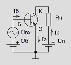
Figure 21 - Scheme with a common emitter transistor n-p-n
The stage gain is equal to the ratio of the collector current to the base current and can usually reach from tens to several hundreds. A transistor connected according to a common emitter circuit can theoretically give the maximum signal amplification in terms of power, relative to other options for turning on the transistor. The input impedance of the stage under consideration, equal to the ratio of the base-emitter voltage to the base current, ranges from hundreds to thousands of ohms. This is less than that of a cascade with a transistor connected in a common collector circuit. The output signal of the common-emitter stage has a phase shift of 180° relative to the input signal. Temperature fluctuations have a significant impact on the operation mode of a transistor connected according to a common emitter circuit, and therefore special temperature stabilization circuits should be used. Due to the fact that the resistance of the collector junction of the transistor in the considered cascade is higher than in the cascade with a common base, more time is needed for the recombination of charge carriers, and, consequently, the cascade with a common emitter has a worse frequency property.
A load is connected to the emitter of a transistor connected according to a common collector circuit, and an input signal is applied to the base. The input current to the stage is the base current of the transistor, and the output current is the emitter current. This is reflected in Figure 22, which shows the switching circuit of a bipolar p-n-p transistor.
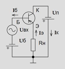
Figure 22 - Scheme with a common collector p-n-p transistor
An output signal is taken from a load resistor connected in series with the emitter output. The input of the stage has a high resistance, usually from tenths of a megaohm to a few megaohms, due to the fact that the collector junction of the transistor is locked. And the output impedance of the cascade, on the contrary, is small, which makes it possible to use such cascades to match the previous cascade with the load. A cascade with a transistor connected according to a common collector circuit does not amplify the voltage, but amplifies the current (usually 10 ... 100 times). The phase of the input voltage of the signal applied to the stage coincides with the phase of the output voltage, i.e. there is no inversion. It is because of the conservation of the phase of the input and output signal that the cascade with a common collector has a different name - an emitter follower. The temperature and frequency properties of the emitter follower are worse than those of a cascade in which the transistor is connected according to a common base circuit.
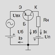
Figure 23 - Scheme with a common base transistor p-n-p
In a cascade assembled according to a common base circuit, the input signal voltage is applied between the emitter and the base of the transistor, and the output voltage is removed from the collector-base terminals. Turning on the transistor p-n-p structure according to the circuit with a common base is shown in Figure 23.
In this case, the emitter junction of the component is open and its conductivity is high. The input impedance of the cascade is small and usually ranges from a few to hundreds of ohms, which is attributed to the disadvantage of the described switching on of the transistor. In addition, for the operation of the cascade with a common-base transistor, two separate power supplies are required, and the cascade current gain is less than unity. The voltage gain of the cascade often reaches from tens to several hundred times.
The advantages include the possibility of the cascade functioning at a significantly higher frequency compared to the other two options for switching on the transistor, and the weak effect of temperature fluctuations on the operation of the cascade. That is why cascades with transistors connected according to a common base circuit are often used to amplify high-frequency signals.
A phototransistor is a transistor that is sensitive to the light flux irradiating it. Usually, a discrete phototransistor is similar in design to a discrete transistor, with the difference that in the sealed case of the phototransistor there is a window, for example, made of glass or transparent special plastic, through which radiation enters the base region of the phototransistor. The inclusion of a phototransistor in an electrical circuit is such that the positive pole of an external power source is connected to the emitter, a load resistor is connected to the collector, to which, in turn, the negative pole of the power source is connected. When the base region is irradiated, charge carriers are generated. The highest concentration of majority charge carriers will be in the base, which will lead to the opening of the phototransistor, and minority charge carriers will migrate to the collector junction. Therefore, irradiation of the phototransistor leads to an increase in its collector current. The greater the illumination of the base area, the more significant the collector current of the phototransistor will become. Thus, the phototransistor can be controlled both as a conventional bipolar transistor, by varying the base current, and as a light-sensitive device. The important parameters of a phototransistor include dark current, illumination current, and integral sensitivity. Dark current is the collector current in the absence of irradiation. Illumination current is the collector current in the presence of irradiation. Integral sensitivity is the ratio of the collector current of the connected phototransistor to the value of the luminous flux.
Phototransistors are used in optocouplers, automation and telecontrol devices, street lighting devices, etc.