Star News


An electronic key on a transistor - the principle of operation and the circuit. Transistor key circuit and operation.
The transistor switch is the main component in the pulse converter technology. In the schemes of all impulse sources nutrition, which almost completely replaced transformer sources power supply, transistor switches are used. Examples of such power supplies are computer blocks power supplies, chargers for phones, laptops, tablets, etc. Transistor keys have replaced electromagnetic relays, since they have such a main advantage as the absence of mechanical moving parts, which increases the reliability and durability of the key. In addition, the speed of turning on and off electronic semiconductor switches is much higher than the speed of electromagnetic relays.
Also, a transistor switch is often used to turn on / off (switch) a load of significant power at the signal of the microcontroller.
The essence of the electronic key is to control it with high power by a low power signal.
There are semiconductor switches based on transistors, thyristors, triacs. However, this article discusses the operation of an electronic key on a bipolar transistor. In subsequent articles, other types of semiconductor switches will be considered.
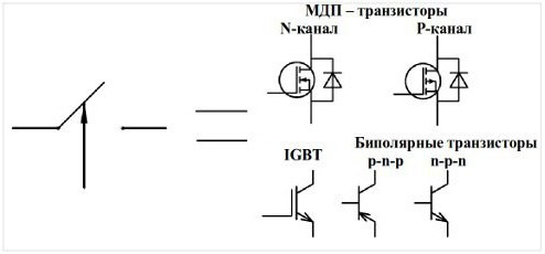
Depending on the semiconductor structure, bipolar transistors are divided into two types: p — n — p and n — p — n type ( rice. one ).
Rice. 1 - Structures of bipolar transistors
In the circuits, bipolar transistors are designated as shown in rice. 2 . The middle terminal is called the base, the terminal with the “arrow” is the emitter, the remaining terminal is the collector.
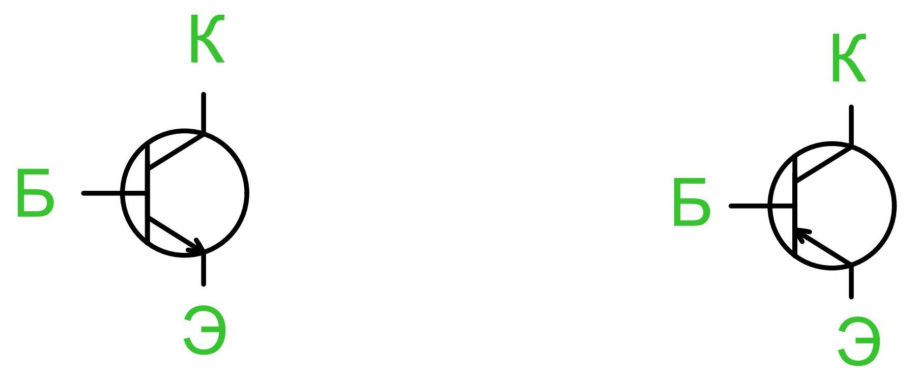
Rice. 2 - Designation of transistors in circuits
Also, transistors can be conditionally depicted in the form of two diodes, which are connected back to back, their junction will always be the base ( fig.3 ).
Rice. 3 - Schemes for replacing transistors with diodes
transistor key. Inclusion schemes.
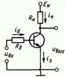
Switching circuits for transistors of various semiconductor structures are shown in rice. 4 . The junction between the base and the emitter is called the emitter junction, and the junction between the base and the collector is called the collector junction. To turn on (open) the transistor, it is necessary that the collector junction be biased in the opposite direction, and the emitter - in the forward direction.
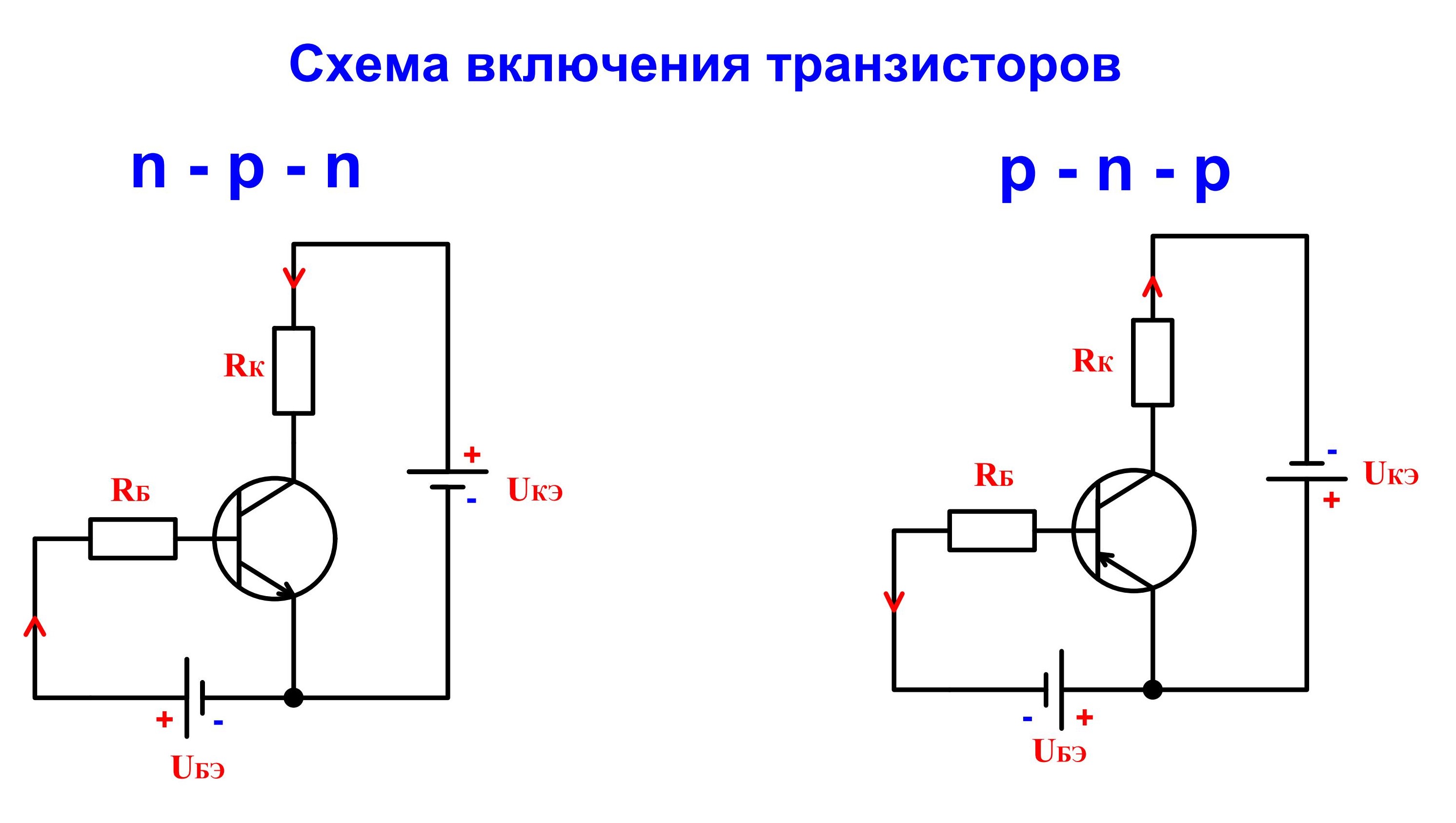
Rice. 4 - Transistor key. Switching schemes
Power supply voltage U un applied to collector and emitter terminals U ke through a load resistor R to (cm. rice. 4 ). Control voltage (control signal) is applied between base and emitter U bae through a current limiting resistor R b .
When the transistor operates in the key mode, it can be in two states. The first is cutoff mode. In this mode, the transistor is completely closed, and the voltage between the collector and emitter is equal to the voltage of the power supply. The second state is saturation mode. In this mode, the transistor is fully on, and the voltage between the collector and emitter is equal to the voltage drop across p — n - transitions and for various transistors is in the range from hundredths to tenths of a volt.
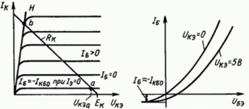
On the load direct input static characteristics of the transistor ( rice. five ) the saturation region is on the segment 1-2 , and the cutoff region on the segment 3-4 . The intermediate region between these segments is the region 2-3 called the active region. It is guided when the transistor operates in amplifier mode.
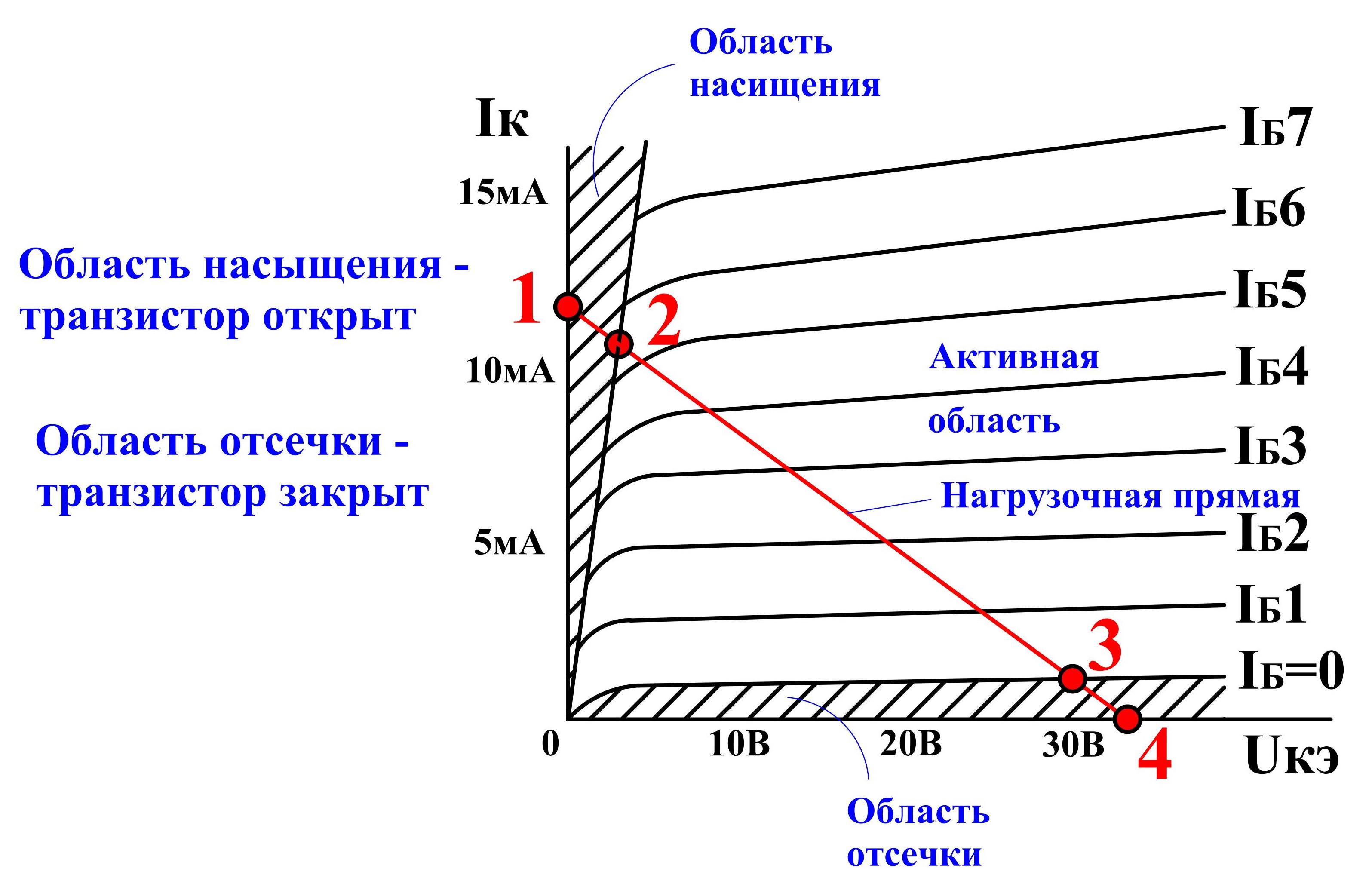
Rice. 5 - Input static characteristic of the transistor
In order to make it easier to remember the polarity of connecting the power supply and control signal voltage, pay attention to the emitter arrow. It indicates the direction of current flow ( fig.6 ).
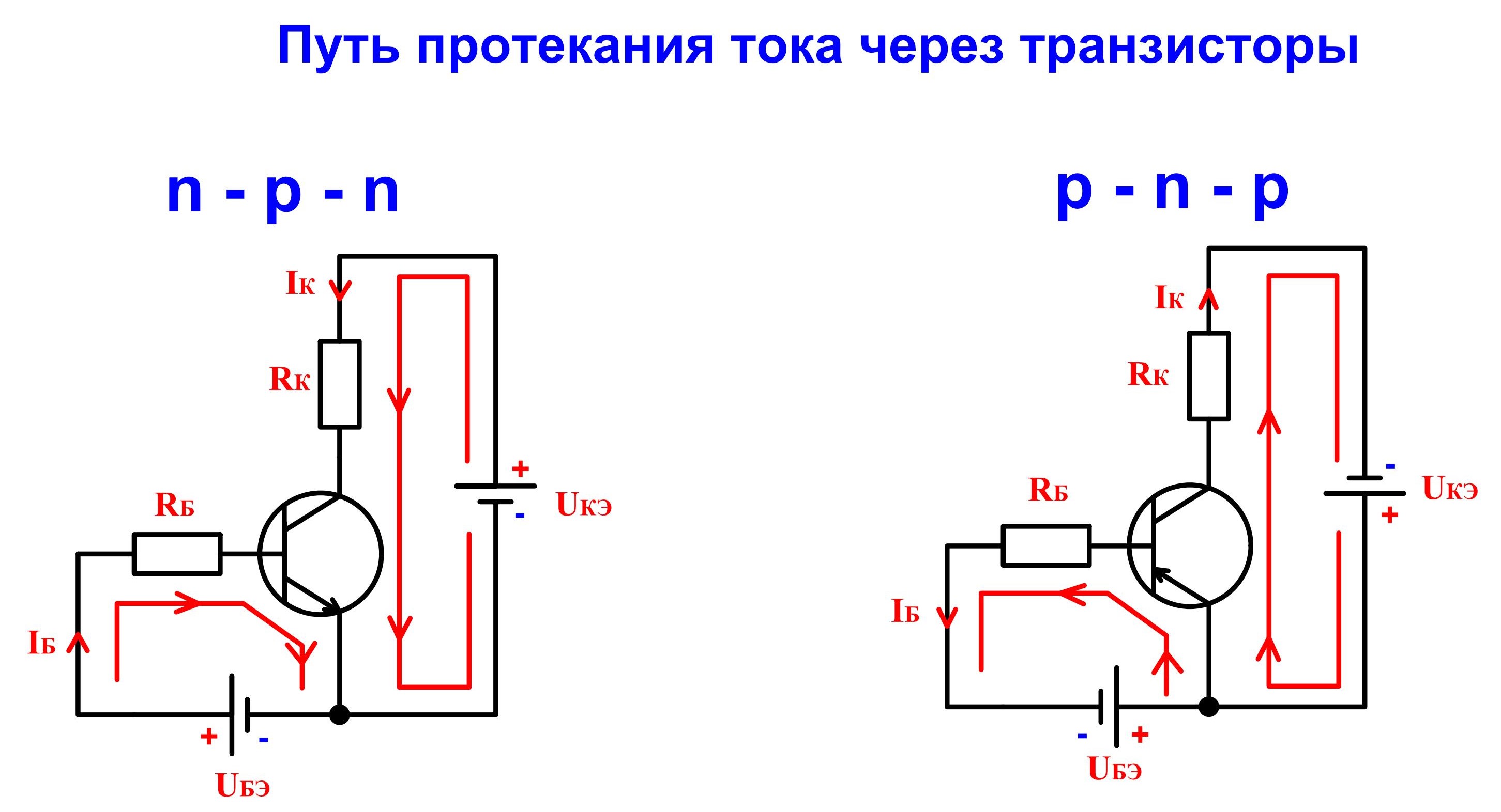
Rice. 6 - The path of current flow through the transistor switch
Calculation of transistor switch parameters
For an example of the operation of a key, we will use an LED as a load. Its connection diagram is shown in rice. 7 . Pay attention to the polarity of connecting power supplies and the LED in transistors of different semiconductor structures.
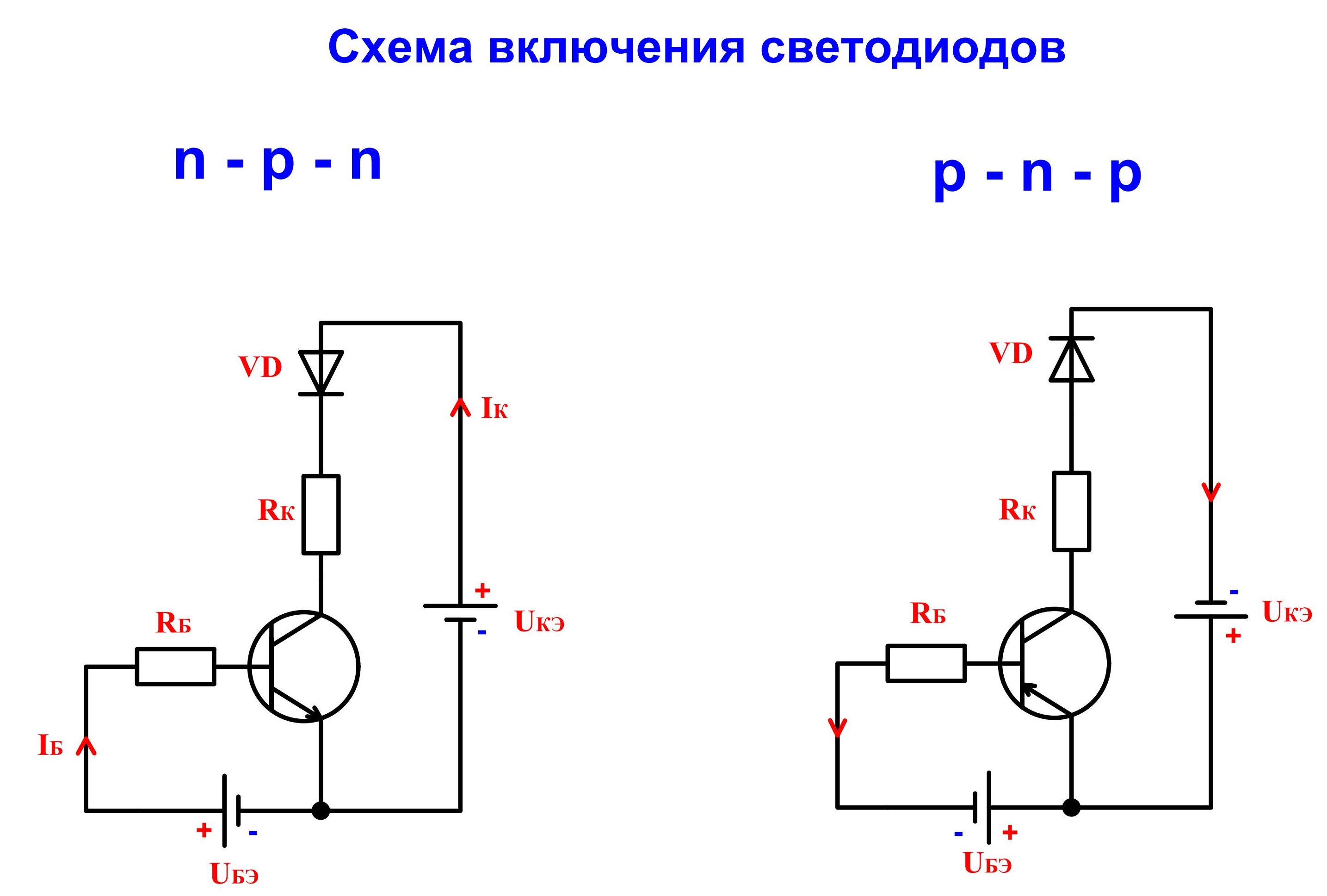
Rice. 7 - Schemes for connecting an LED to transistor switches
Let's calculate the main parameters of a transistor switch made on a transistor n — p — n type. Let's have the following initial data:
- voltage drop across the LED Δ UVD = 2 V;
- rated current of the LED IVD= 10 mA;
- power supply voltage Uun(marked on the diagram Uke) = 9 V;
- input signal voltage Usun= 1.6 V.
Now let's look again at the diagram shown in rice. 7 . As we can see, it remains to determine the resistance of the resistors in the base and collector circuits. The transistor can choose any bipolar corresponding semiconductor structure. Take for example the Soviet transistor n — p — n type MP111B.
Calculation of resistance in the transistor collector circuit
The resistance in the collector circuit is designed to limit the current that flows through the LED. VD , as well as for overload protection of the transistor itself. Since when the transistor opens, the current in its circuit will be limited only by the resistance of the LED VD and resistor R to .
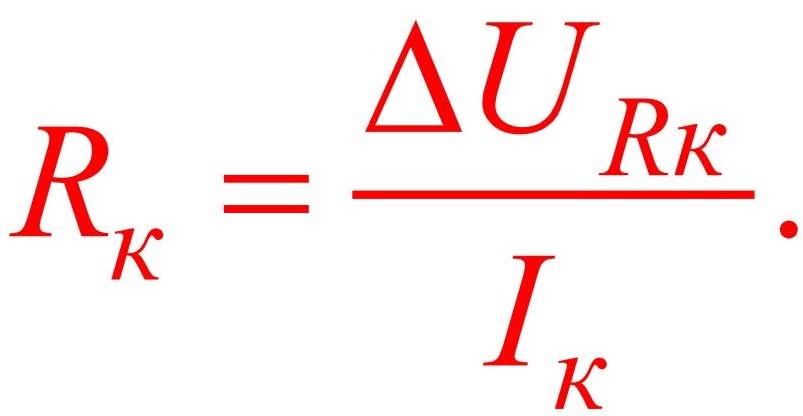
Let's define the resistance R to . It is equal to the voltage drop across it Δ U R to divided by the current in the collector circuit I to :
So the collector was set by us initially, - this is the rated current of the LED. It must not exceed I k=10mA .
Now find the voltage drop across the resistor R to . It is equal to the power supply voltage U un (U ke ) minus the voltage drop across the LED Δ U VD and minus the voltage drop across the transistor ΔU ke :
The voltage drop on the LED, as well as the voltage of the power source, are initially set and equal to 0.2V and 9V, respectively. The voltage drop for the MP111B transistor, as well as for other Soviet transistors, is taken to be about 0.2 V. For modern transistors (for example, BC547, BC549, N2222 and others), the voltage drop is about 0.05 V and lower.
The voltage drop across the transistor can be measured when it is fully on, between the collector and emitter terminals, and further correct the calculation. But, as we will see later, the collector resistance can be chosen by a simpler method.
The resistance in the collector circuit is:
Calculation of resistance in the transistor base circuit
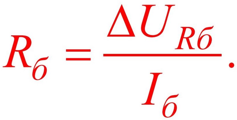
Now we need to determine the resistance of the base R b . It is equal to the voltage drop across the resistance itself. ΔURb divided by base current I b :
The voltage drop across the base of the transistor is equal to the input signal voltage Uvs minus the voltage drop across the base-emitter junction ΔUbe . The input signal voltage is set in the initial data and is equal to 1.6 V. The voltage drop between the base and the emitter is about 0.6 V.
Next, find the base current Ib . It is equal to the collector current Ib divided by the current gain of the transistor β . The gain for each transistor is given in datasheets or in reference books. Even easier to know the meaning β you can use a multimeter. Even the simplest multimeter has such a function. For this transistor β=30 . For modern transistors β equal to about 300 ... 600 units.
Now we can find the required base resistance.
Thus, using the above methodology, you can easily determine the required resistor values in the base and collector circuits. However, it must be remembered that the calculated data does not always allow you to accurately determine the resistor values. Therefore, it is better to perform a finer adjustment of the key experimentally, and calculations are necessary only for the initial estimate, that is, they help to narrow the range of choice of resistor values.
To determine the values of the resistors, you need to turn on a variable resistor in series with the base and collector resistors and, by changing its value, obtain the necessary values \u200b\u200bof the base and collector currents ( rice. eight ).
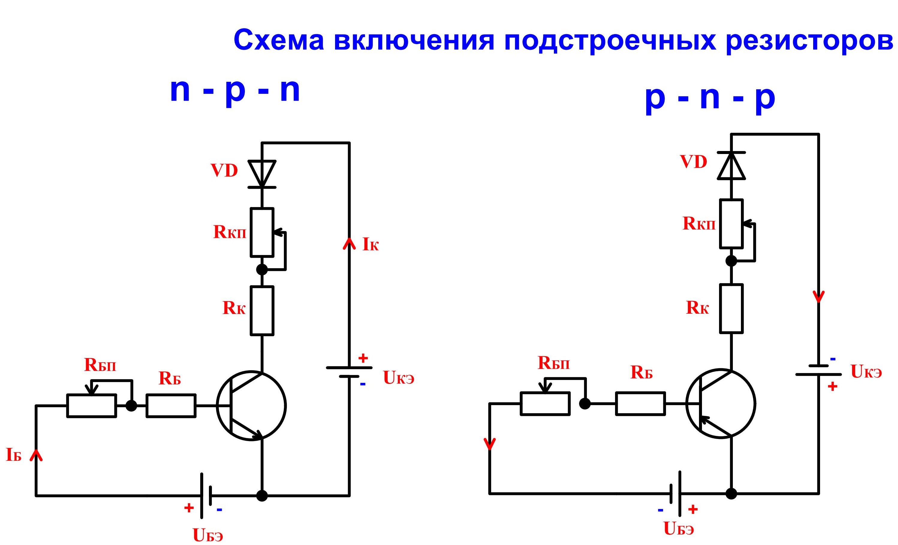
Rice. 8 - Scheme for switching on variable resistors
Recommendations for choosing transistors for electronic keys
- Also, the voltage at the base in saturation mode should not be lower than the minimum value, otherwise the transistor switch will work unstably.
The nominal voltage between the collector and the emitter, which is specified by the manufacturer, must be higher than the voltage of the power supply.
The nominal collector current, which is also specified by the manufacturer, must be greater than the load current.
It is necessary to ensure that the current and voltage of the base of the transistor do not exceed the allowable values.
What load are you talking about? Yes, about any - relays, light bulbs, solenoids, motors, several LEDs at once or a heavy-duty power LED spotlight. In short, everything that consumes more than 15mA and / or requires a supply voltage of more than 5 volts.
Take, for example, a relay. Let it be BS-115C. The winding current is about 80mA, the winding voltage is 12 volts. The maximum contact voltage is 250V and 10A.
Connecting a relay to a microcontroller is a task that almost everyone had. One problem is that the microcontroller cannot provide the power necessary for the normal operation of the coil. The maximum current that the controller output can pass through rarely exceeds 20mA, and this is still considered cool - a powerful output. Usually no more than 10mA. Yes, the voltage here is not higher than 5 volts, and the relay needs as many as 12. There are, of course, relays for five volts, but the current is consumed twice as much. In general, where the relay does not kiss - everywhere the ass. What to do?
The first thing that comes to mind is to put a transistor. The right decision - a transistor can be selected for hundreds of milliamps, or even amperes. If one transistor is missing, then they can be turned on in cascades, when a weak one opens a stronger one.
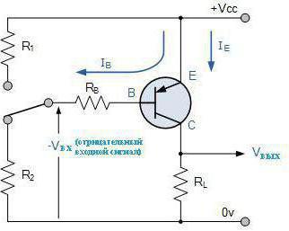
Since we have assumed that 1 is on and 0 is off (this is logical, although it contradicts my old habit that came from the AT89C51 architecture), then 1 will supply power, and 0 will remove the load. Let's take a bipolar transistor. The relay requires 80mA, so we are looking for a transistor with a collector current of more than 80mA. In imported datasheets, this parameter is called I c, in ours I k. The first thing that came to mind is KT315 - a masterpiece soviet transistor that was used almost everywhere :) Such an orange one. It costs no more than one ruble. It will also run KT3107 with any letter index or imported BC546 (as well as BC547, BC548, BC549). In a transistor, first of all, it is necessary to determine the purpose of the conclusions. Where is the collector, where is the base, and where is the emitter. It is best to do this according to the datasheet or reference book. Here is an example from the datasheet:
If you look at its front side, the one with the inscriptions, and keep the legs down, then the conclusions, from left to right: Emitter, Collector, Base.
We take a transistor and connect it according to the following scheme:
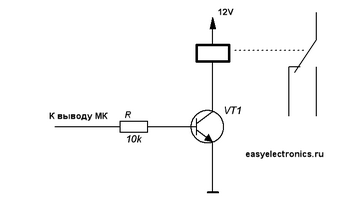 |
The collector to the load, the emitter, the one with the arrow, to the ground. And the base to the output of the controller.
A transistor is a current amplifier, that is, if we pass a current through the Base-Emitter circuit, then a current equal to the input multiplied by the gain h fe can pass through the Collector-Emitter circuit.
h fe for this transistor is several hundred. Something like 300, I don't remember exactly.
The maximum output voltage of the microcontroller when applied to the unity port = 5 volts (the voltage drop of 0.7 volts at the Base-Emitter junction can be neglected here). The resistance in the base circuit is 10,000 ohms. This means that the current, according to Ohm's law, will be equal to 5/10000=0.0005A or 0.5mA - a completely insignificant current from which the controller will not even sweat. And the output at this point in time will be I c \u003d I be * h fe \u003d 0.0005 * 300 \u003d 0.150A. 150mA is more than 100mA, but that just means the transistor will open wide open and put out the most it can. So our relay will receive food in full.
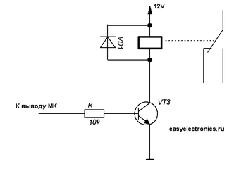
Is everyone happy, is everyone happy? But no, there is a mess here. In a relay, a coil is used as an actuating element. And the coil has a rather strong inductance, so it is impossible to abruptly cut off the current in it. If you try to do this, then the potential energy accumulated in the electromagnet field will come out in another place. At zero break current, this place will be voltage - with a sharp interruption of the current, there will be a powerful surge of voltage on the coil, hundreds of volts. If the current is interrupted by mechanical contact, then there will be an air breakdown - a spark. And if you cut it off with a transistor, then it will simply kill it.
It is necessary to do something, somewhere to put the energy of the coil. Not a problem, close it to yourself by putting a diode. During normal operation, the diode is turned on opposite to the voltage and no current flows through it. And when you turn off the voltage across the inductance will be in the other direction and will pass through the diode.
 |
True, these games with voltage surges in a nasty way affect the stability of the power supply network of the device, so it makes sense to screw in an electrolytic capacitor for another hundred microfarads near the coils between the plus and minus of the power supply. It will take on most of the pulsation.
The beauty! But you can do even better - reduce consumption. The relay has enough high current breaking away, but the holding current of the armature is less than three times. Who cares, but the toad crushes me to feed the coil more than it deserves. This is after all, heating and energy consumption and much more. We also take and insert into the circuit a polar capacitor for a dozen other microfarads with a resistor. What happens now:
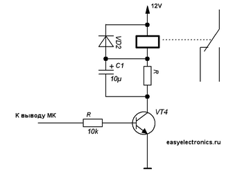 |
When the transistor is opened, the capacitor C2 is not yet charged, which means that at the moment of its charge it is almost a short circuit and the current through the coil goes without restrictions. Not for long, but this is enough to break the relay armature from its place. Then the capacitor will charge and turn into a break. And the relay will be powered through a current limiting resistor. The resistor and capacitor should be selected in such a way that the relay operates clearly.
After the transistor closes, the capacitor is discharged through the resistor. From this follows a counter zapadlo - if you immediately try to turn on the relay, when the capacitor has not yet been discharged, then the current for a jerk may not be enough. So here we need to think at what speed the relay will click. Conder, of course, will be discharged in a split second, but sometimes this is a lot.
Let's add another upgrade.
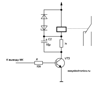
When the relay opens, the energy of the magnetic field is bled off through the diode, but at the same time, current continues to flow in the coil, which means it continues to hold the armature. The time between the removal of the control signal and the falling off of the contact group increases. Zapadlo. It is necessary to make an obstacle to the flow of current, but such that it does not kill the transistor. We plug in a zener diode with an opening voltage below the limiting breakdown voltage of the transistor.
From a piece of datasheet it can be seen that the limiting voltage of the Collector-Base (Collector-Base voltage) for the BC549 is 30 volts. We screw in a 27 volt zener diode - Profit!
As a result, we provide a voltage surge on the coil, but it is controlled and below the critical breakdown point. Thus, we significantly (at times!) Reduce the turn-off delay.
 |
Now you can quite stretch and start painfully scratching your turnips about how to place all this rubbish on a printed circuit board ... We have to look for compromises and leave only what is needed in this circuit. But this is already an engineering flair and comes with experience.
Of course, instead of a relay, you can plug in a light bulb and a solenoid, and even a motor, if it passes through the current. The relay is taken as an example. And, of course, the entire diode-capacitor kit is not required for the light bulb.
Enough for now. Next time I will talk about Darlington assemblies and MOSFET keys.
In pulse devices, transistor keys can often be found. Transistor switches are present in flip-flops, switches, multivibrators, blocking oscillators and other electronic circuits. In each circuit, the transistor key performs its function, and depending on the operating mode of the transistor, the key circuit as a whole may change, however, the main circuit diagram transistor key - the following:
There are several main modes of operation of the transistor switch: normal active mode, saturation mode, cutoff mode and active inverse mode. Although the transistor switch circuit is in principle a common-emitter transistor amplifier circuit, this circuit differs in function and modes from a typical amplifier stage.
In a key application, the transistor serves as a high-speed switch, and the main static states are two: the transistor is closed and the transistor is open. Latched state - the open state when the transistor is in cutoff mode. Closed state - the state of saturation of the transistor, or a state close to saturation, in this state the transistor is open. When the transistor switches from one state to another, this is the active mode, in which the processes in the cascade proceed non-linearly.
Static states are described according to the static characteristics of the transistor. There are two characteristics: the output family - the dependence of the collector current on the collector-emitter voltage and the input family - the dependence of the base current on the base-emitter voltage.
The cutoff mode is characterized by a bias of both p-n junctions of the transistor in the opposite direction, and there is a deep cutoff and a shallow cutoff. Deep cutoff is when the voltage applied to the junctions is 3-5 times higher than the threshold voltage and has the reverse polarity of the working one. In this state, the transistor is open, and the currents of its electrodes are extremely small.
With a shallow cutoff, the voltage applied to one of the electrodes is lower, and the electrode currents are greater than with a deep cutoff, as a result, the currents already depend on the applied voltage in accordance with the lower curve from the output characteristic family, this curve is called the “cutoff characteristic” .
For example, we will carry out a simplified calculation for the key mode of a transistor that will operate on a resistive load. The transistor will be in only one of two main states for a long time: fully open (saturation) or fully closed (cutoff).
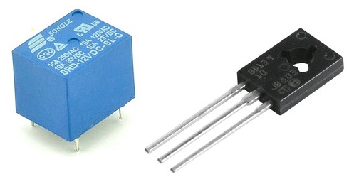
Let the transistor load be the winding of the SRD-12VDC-SL-C relay, the coil resistance of which at a nominal 12 V will be 400 ohms. Let's neglect the inductive nature of the relay winding, let the developers provide a snubber to protect against transient surges, but we will calculate based on the fact that the relay will be turned on once and for a very long time. We find the collector current by the formula:
Ik \u003d (Upit-Ukenas) / Rн.
Where: Ik - D.C. collector; Upit - supply voltage (12 volts); Ukenas - saturation voltage bipolar transistor(0.5 volts); Rн - load resistance (400 Ohm).
We get Ik \u003d (12-0.5) / 400 \u003d 0.02875 A \u003d 28.7 mA.
For fidelity, let's take a transistor with a margin for limiting current and limiting voltage. Suitable BD139 in SOT-32 package. This transistor has the parameters Ikmax = 1.5 A, Ukemax = 80 V. There will be a good margin.
To provide a collector current of 28.7 mA, it is necessary to provide an appropriate base current. The base current is determined by the formula: Ib = Ik / h21e, where h21e is the static current transfer coefficient.
Modern multimeters allow you to measure this parameter, and in our case it was 50. So Ib \u003d 0.0287 / 50 \u003d 574 μA. If the value of the coefficient h21e is unknown, for reliability, you can take the minimum from the documentation for this transistor.
To determine the required value of the base resistor. The base-emitter saturation voltage is 1 volt. So, if the control is carried out by a signal from the output of a logic microcircuit, the voltage of which is 5 V, then to provide the required base current of 574 μA, with a drop at the transition of 1 V, we get:
R1 \u003d (Uin-Ubenas) / Ib \u003d (5-1) / 0.000574 \u003d 6968 Ohm
Let's choose a smaller one (so that there is exactly enough current) from the standard series of a 6.8 kOhm resistor.
BUT, in order for the transistor to switch faster and for the operation to be reliable, we will use an additional resistor R2 between the base and the emitter, and some power will drop on it, which means it is necessary to lower the resistance of the resistor R1. Let's take R2 = 6.8 kOhm and adjust the value of R1:
R1 = (Uin-Ubenas) / (Ib + I (through resistor R2) = (Uin-Ubenas) / (Ib + Ubenas / R2)
R1 \u003d (5-1) / (0.000574 + 1/6800) \u003d 5547 ohms.
Let it be R1 = 5.1 kOhm, and R2 = 6.8 kOhm.
Let's calculate the losses on the key: P \u003d Ik * Ukenas \u003d 0.0287 * 0.5 \u003d 0.014 W. The transistor does not need a heatsink.
The transistor key is the main element of digital electronics devices and very many power electronics devices. The parameters and characteristics of the transistor switch to a very large extent determine the properties of the corresponding circuits.
Keys on bipolar transistors . The simplest key on a bipolar transistor, connected according to the common emitter circuit, and the corresponding timing diagram of the input voltage are shown in fig. 14.5.
Rice. 14.5. Bipolar transistor key
Consider the operation of a transistor switch in steady state. Until the point in time t 1 the emitter junction of the transistor is off and the transistor is in cutoff mode. In this mode i to =– i b =I to (I to- collector reverse current), i uh≈ 0. u R b ≈u R to ≈ 0;u bae ≈ –U 2 ;u ke ≈–E to .
In the span of time t 1 …t 2 the transistor is open. In order for the voltage across the transistor u ke was minimal, stress U 1 usually chosen so that the transistor is either in saturation mode, or in the border mode, very close to saturation mode.
Keys on field-effect transistors have low residual stress. They can switch weak signals (in units of microvolts and less). This is a consequence of the fact that the output characteristics of field-effect transistors pass through the origin.
For example, let's depict the output characteristics of a transistor with a control transition and a channel p-type in the area adjacent to the origin (Fig. 14.6).
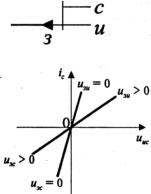
Rice. 14.6. FET with p-channel
Note that the characteristics in the third quadrant correspond to the given voltages between the gate and the drain.
In a static state, the FET switch consumes very little control current. However, this current increases as the switching frequency increases. A very large input resistance of field-effect transistor keys actually provides galvanic isolation of the input and output circuits. This eliminates the need for transformers in the control circuits.
On fig. 14.7 shows a diagram of a digital key on an MIS transistor with an induced channel n-type and resistive load and corresponding timing diagrams.
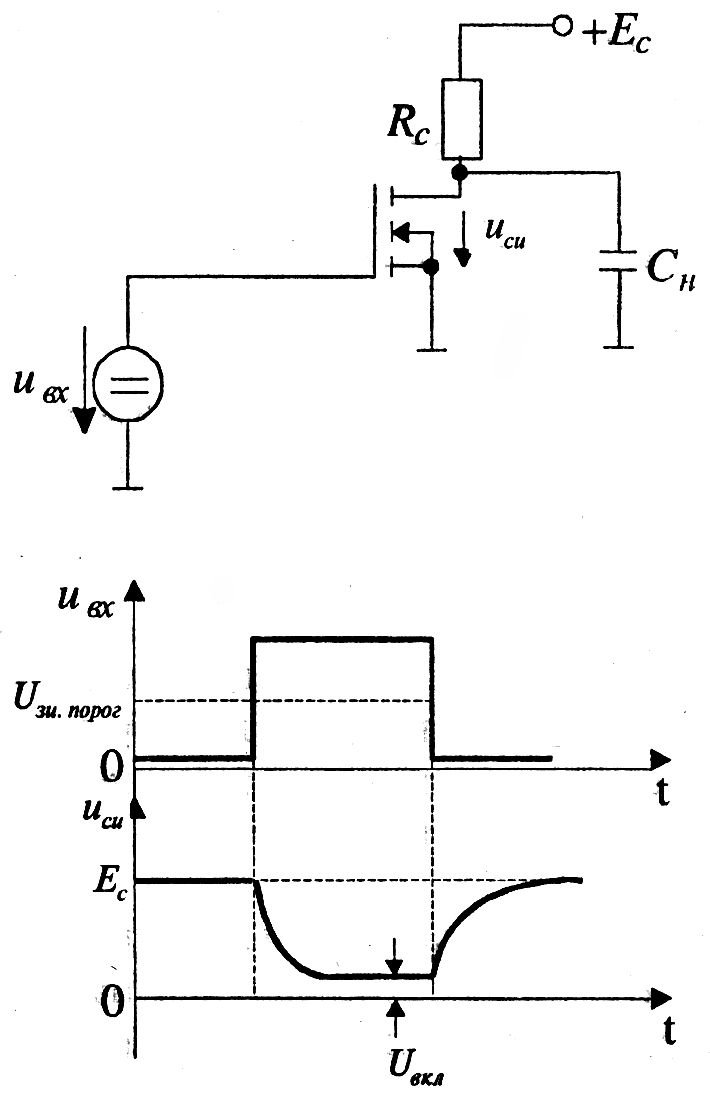
Rice. 14.7. FET digital key
The diagram shows the load capacity With n, modeling the capacitance of devices connected to a transistor switch. Obviously, when the input signal is zero, the transistor is off and u si =E with. If the voltage uin is greater than the threshold voltage U z.threshold transistor, it opens and the voltage u si decreases.
Logic elements
A logical element (logic gate) is an electronic circuit that performs some simple logical operation. On fig. 14.8 shows examples of conventional graphic symbols for some logical elements.
Rice. 14.8. Logic elements
The logic element may be implemented as a separate integrated circuit. Often an integrated circuit contains several logic elements.
Logic gates are used in digital electronics devices (logic devices) to perform simple conversion of logic signals.
Classification of logical elements. The following classes of logical elements (the so-called logics) are distinguished:
resistor-transistor logic (TRL);
diode-transistor logic (DTL);
transistor-transistor logic (TTL);
emitter-transistor logic (ESL);
transistor-transistor logic with Schottky diodes (TTLSh);
R(R- TIR);
MOSFET-based logic with type channels n(n- TIR);
logic based on complementary keys on MIS transistors (CMOS, CMOS);
integral injection logic I 2 L;
logic based on GaAs gallium arsenide semiconductor.
Currently, the following logics are most widely used: TTL, TTLSH, CMOS, ESL. Logic elements and other digital electronic devices are produced as part of a series of microcircuits: TTL - K155, KM155, K133, KM133; TTLSh - 530, KR531, KM531, KR1531, 533, K555, Km555, 1533, KR1533; ESL - 100, K500, K1500; CMOS - 564, K561, 1564, KR1554; GaAs - K6500.
The most important parameters of logic elements:
Performance is characterized by the signal propagation delay time t sp and maximum operating frequency F Max. The delay time is usually determined by level differences 0.5 U in and 0.5Δ U exit. Maximum operating frequency F Max is the frequency at which the circuit remains operational.
The load capacity is characterized by the input pooling factor To about (sometimes the term "output pooling factor" is used). Value To about is the number of logical inputs, the value To once- the maximum number of the same type of logical elements that can be connected to the output of this logical element. Their typical meanings are: To about =2…8,To once=4…10. For elements with increased load capacity To once =20…30.
Noise immunity in static mode is characterized by voltage U pst, which is called static noise immunity. This is the maximum allowable static noise voltage at the input, at which there is still no change in the output levels of the logic element.
The power consumed by the microcircuit from the power source. If this power is different for two logical states, then the average power consumption for these states is often indicated.
Supply voltage.
High and low level input threshold voltages U in.1threshold and U input.0threshold, corresponding to a change in the state of the logical element.
High and low output voltages U out1 and U out0 .
Other parameters are also used.
Features of logical elements of various logics. A specific series of microcircuits is characterized by the use of a typical electronic assembly - a basic logic element. This element is the basis for building a wide variety of digital electronic devices.
Base element TTL contains a multi-emitter transistor that performs a logical AND operation, and a complex inverter (Fig. 14.9).
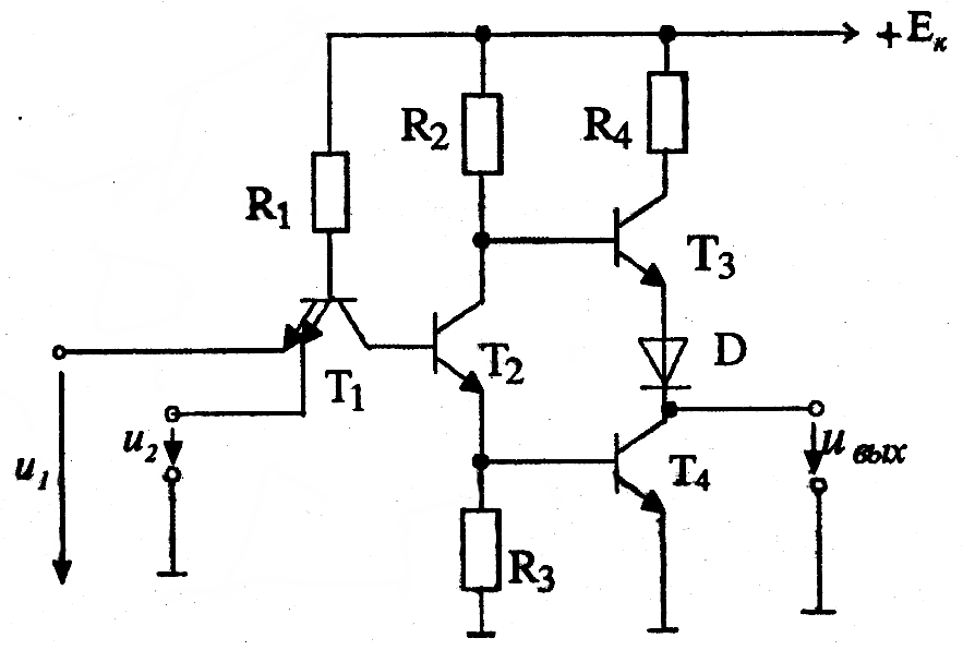
Rice. 14.9. Base element TTL
If a low voltage level is simultaneously applied to one or both inputs, then the multi-emitter transistor is in saturation and the transistor T 2 is closed, and therefore the transistor T 4 is also closed, i.e. the output will have a high voltage level. If a high voltage level simultaneously operates on both inputs, then the transistor T 2 opens and enters saturation mode, which leads to the opening and saturation of the transistor T 4 and the locking of the transistor T 3, i.e. the AND-NOT function is implemented. To increase the speed of TTL elements, transistors with diodes or Schottky transistors are used.
Basic logic element TTLSH (on the example of the K555 series). The element
AND-NOT (Fig. 14.10, a), and in Fig. 14.10, b shows a graphical representation of the Schottky transistor.
![]()
Rice. 14.10. Logic element TTLSH
Transistor VT4 is a conventional bipolar transistor. If both input voltages u in1 and u vx2 have a high level, then the diodes VD3 and VD4 are closed, the transistors VT1, VT5 are open and the output voltage is low. If at least one input has a low-level voltage, then the transistors VT1 and VT5 are closed, and the transistors VT3 and VT4 are open, and a low-level voltage occurs at the input. TTLSh microcircuits of the K555 series are characterized by the following parameters:
supply voltage +5 AT;
low level output voltage not more than 0.4 AT;
high level output voltage not less than 2.5 AT;
noise immunity - not less than 0.3 V;
average propagation delay time 20 ns;
maximum operating frequency 25 MHz.
Features of other logics. The basis of the basic logical element of the ESL is a current switch, the circuit of which is similar to that of a differential amplifier. The ESL chip is powered by a negative voltage (-4 AT for K1500 series). The transistors of this microcircuit do not enter saturation mode, which is one of the reasons for the high speed of the ESL elements.
In microcircuits n-MOS and p-MOS switches are used respectively on MOSFETs with n-channels and dynamic load and on MOSFETs with p-channel. Complementary MIS logic elements (CMOS or CMOS logic) are used to eliminate the power consumption of the logic element in the static state.
Logic based on the GaAs gallium arsenide semiconductor is characterized by the highest speed, which is a consequence of the high electron mobility (3...6 times higher compared to silicon). Chips based on GaAs can operate at frequencies of the order of 10 GHz.
When working with complex circuits, it is useful to use various technical tricks that allow you to achieve your goal with little effort. One of them is the creation of transistor switches. What are they? Why should they be created? Why are they also called "electronic keys"? What are the features of this process and what should be paid attention to?
What are transistor switches made of?
They are performed using field or First ones are further divided into MIS and keys, which have a control pn junction. Among bipolar ones, non-saturated ones are distinguished. A 12 Volt transistor key will be able to satisfy basic requests from a radio amateur.
Static mode of operation
 It analyzes the private and public state of the key. The first input contains a low voltage level, which indicates a logic zero signal. In this mode, both transitions are in the opposite direction (a cutoff is obtained). And only thermal can affect the collector current. In the open state, at the input of the key there is a high voltage level corresponding to the logical unit signal. It is possible to work in two modes simultaneously. Such performance may be in the saturation region or the linear region of the output characteristic. We will dwell on them in more detail.
key saturation
In such cases, the transistor junctions are forward biased. Therefore, if the base current changes, then the collector value will not change. In silicon transistors, approximately 0.8 V is needed to obtain a bias, while for germanium transistors, the voltage fluctuates within 0.2-0.4 V. How is key saturation achieved in general? This increases the base current. But everything has its limits, as does increasing saturation. So, when a certain current value is reached, it stops increasing. And why carry out key saturation? There is a special coefficient that displays the state of affairs. With its increase, the load capacity that transistor switches have increases, destabilizing factors begin to influence with less force, but performance deteriorates. Therefore, the value of the saturation coefficient is chosen from compromise considerations, focusing on the task that will need to be performed.
Disadvantages of an unsaturated key
 And what happens if the optimal value has not been reached? Then there will be such disadvantages:
- The voltage of the public key will drop and lose to about 0.5 V.
- The noise immunity will deteriorate. This is due to the increased input resistance that is observed in the keys when they are in the open state. Therefore, interference like power surges will also lead to a change in the parameters of transistors.
- A saturated key has significant temperature stability.
As you can see, this process is still better to carry out in order to ultimately get a more advanced device.
Performance
Interaction with other keys
 To do this, elements of communication are used. So, if the first key at the output has a high voltage level, then the second one opens at the input and works in the specified mode. And vice versa. Such a communication circuit significantly affects the transient processes that occur during switching and the speed of the keys. This is how a transistor switch works. The most common are circuits in which the interaction takes place only between two transistors. But this does not mean at all that this cannot be done by a device in which three, four or even more elements will be used. But in practice, it is difficult to find an application for this, so the operation of a transistor switch of this type is not used.
What to choose
 What is better to work with? Let's imagine that we have a simple transistor switch, the supply voltage of which is 0.5 V. Then, using an oscilloscope, it will be possible to record all changes. If the collector current is set to 0.5mA, then the voltage will drop by 40mV (there will be approximately 0.8V at the base). By the standards of the task, we can say that this is a rather significant deviation, which imposes a restriction on the use in a whole series of circuits, for example, in switches. Therefore, they use special ones where there is a control pn junction. Their advantages over bipolar counterparts are:
- Insignificant value of residual voltage on the key in the wiring condition.
- High resistance and, as a result, a small current that flows through a closed element.
- Low power is consumed, so a significant source of control voltage is not needed.
- It is possible to switch electrical signals of low level, which are units of microvolts.
Transistor key relay - here is the ideal application for the field. Of course, this message is posted here solely so that readers have an idea of their application. A little knowledge and ingenuity - and the possibilities of implementations in which there are transistor switches, a great many will be invented.
Work example
Let's take a closer look at how a simple transistor switch functions. The switched signal is transmitted from one input and removed from another output. To lock the key, a voltage is applied to the gate of the transistor, which exceeds the values of the source and drain by a value greater than 2-3 V. But you should be careful not to go beyond the permissible range. When the key is closed, its resistance is relatively large - more than 10 ohms. This value is obtained due to the fact that the reverse bias current also affects p-n junction. In the same state, the capacitance between the switched signal circuit and the control electrode fluctuates in the range of 3-30 pF. Now let's open the transistor switch. The circuit and practice will show that then the voltage of the control electrode will approach zero, and is highly dependent on the load resistance and the switched voltage characteristic. This is due to the whole system of interactions of the gate, drain and source of the transistor. This creates certain problems for operation in interrupter mode.
As a solution to this problem, various circuits have been developed that provide voltage stabilization that flows between the channel and the gate. Moreover, due to the physical properties, even a diode can be used in this capacity. To do this, it should be included in the forward direction of the blocking voltage. If the necessary situation is created, the diode will close, and the p-n junction will open. So that when the switched voltage changes, it remains open and the resistance of its channel does not change, a high-resistance resistor can be connected between the source and the input of the key. And the presence of a capacitor will significantly speed up the process of recharging the tanks.
Transistor key calculation
![]() For understanding, I give an example of the calculation, you can substitute your data:
For understanding, I give an example of the calculation, you can substitute your data:
1) Collector-emitter - 45 V. Total power dissipation - 500 mw. Collector-emitter - 0.2 V. Limiting frequency of operation - 100 MHz. Base emitter - 0.9 V. Collector current - 100 mA. Statistical current transfer ratio - 200.
2) Resistor for 60 mA current: 5-1.35-0.2 = 3.45.
3) Collector resistance rating: 3.45\0.06=57.5 Ohm.
4) For convenience, we take a nominal value of 62 ohms: 3.45 \ 62 \u003d 0.0556 mA.
5) We consider the base current: 56 \ 200 \u003d 0.28 mA (0.00028 A).
6) How much will be on the base resistor: 5 - 0.9 \u003d 4.1V.
7) Determine the resistance of the base resistor: 4.1 \ 0.00028 \u003d 14.642.9 ohms.
Conclusion
And finally, about the name "electronic keys". The fact is that the state changes under the influence of current. And what does he represent? That's right, the totality of electronic charges. This is where the second name comes from. That's all. As you can see, the principle of operation and the arrangement of transistor switches are not something complicated, so understanding this is a feasible task. It should be noted that even the author of this article needed to use some reference literature to refresh his own memory. Therefore, if you have questions about terminology, I suggest remembering the availability of technical dictionaries and searching for new information about transistor switches there.