Star News


Oh schemes. Operational amplifier? It's very simple
Good day. In the last article I talked about nutrition. In this article, I will talk about the use Op-amp in linear circuits.
Voltage follower
The first circuit that I will talk about is the unity gain amplifier circuit (unity amplifier) or the so-called. The circuit of this amplifier is shown below.
It is advisable to use dual potentiometers for inputs 1, 2 and 3 - to adjust the left and right channels at the same time. For operational amplifiers, we mean amplifiers that have the following characteristics. At this time, the electrical industry makes the whole range of operational amplifiers integrated design, so their use has reached the level of use of common parts. Most of these op amps have two inputs.
Inverted Input - An input signal to this input appears at the output of a 180° phase-shifter. No reverse input - the signal from this input will be converted to output in the same phase. For operational amplifiers, we use the following circuits. Circuits to set the operating rest point - resistors are used or compensated transistor connections are used.
Unity gain amplifier (voltage follower).
This circuit is a modification, the difference is that there is no feedback resistor and a resistor at the inverting input. Thus, the voltage from the output of the op-amp is completely supplied to the inverting input of the op-amp, and, consequently, the feedback transfer coefficient is equal to one (β = 1).
Circuits for suppressing drift drives and differential components of differential inputs. Differential amplifiers are used at the inputs of operational amplifiers. This is such a transistor connection that will allow you to output a signal to two inputs. The basic layout of the symmetrical differential amplifier is shown in Fig.
The main location of the section is different. increased. The operating points of the transistors are set so that both transistors are in a conducting state. For connections, we highlight two scenarios. Bevel indices are derived from English nouns. The hazy quality of a differential amplifier is the so-called inhibition of the sense signal referred to, denoted in dB, and the value of H is greater the higher the gain.
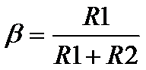
As you know, the input impedance of an op-amp with feedback is determined by the following expression
![]()
- where R BX is the input impedance of the OS without OS,
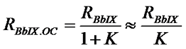
Then for the voltage follower, the input resistance will look like
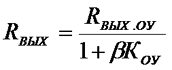
The output impedance of the feedback op amp is the following expression
The resulting differential amplifier voltages are coupled. Basic connection of operational amplifiers. The basic operation of op amps is based on inverting and non-inverting connections. The inverting wiring is shown in fig. It can be seen that at a very large limit, the switching of the inverting inputs is only the reverse and input impedance and is independent of unstable amplifiers. Feedback should always be directed to the inverting input to make it unbeatable.
The network connection is shown in fig. We admit the input signal to the reverse input. Again, we are rising from the balance of the voltages on both inputs. In non-inverse connections, the input voltage does not rotate and the height is always greater than or equal to. The use of operational amplifiers.
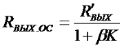
- where R BYX is the input impedance of the OS without OS,
- β is the transmission coefficient of the OS circuit,
- K is the gain of the OS without OS.
Since the voltage follower has a feedback transfer coefficient equal to one (β = 1), the output resistance will have the following form
Applications such as inverted and non-inverted amplifiers are shown to be elevated. Other options. Possible connection schemes are shown in fig. The advantage of these connections, which use both inverse and non-inverting connections, is that the reference source is limited. direct current, and the reverse voltage can be set to the desired output voltage level.
Possible connections are again shown in fig. The amplifier regulates the output voltage so that a current equal to the input current always flows. In the first two connections, it is also closely coupled to the reverse link circuit. Unfortunately, neither end of the lot should be grounded. This disadvantage eliminates the participation of the third.
An example of calculating the parameters of a voltage follower
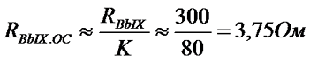
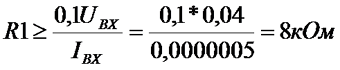
For example, let's calculate the voltage follower on the op-amp, which has a gain of K U = 80 (38 dB) at the required frequency, input impedance R BX = 500 kOhm, output impedance R BYX = 300 Ohm.
Summation is performed at one input. The ratio is applied to the voltage output. The behavior of the characteristic curve is shown in fig. The connection diagram is shown in fig. Transfer overridden. The frequency transmission frequency is shown in fig. These values are used for the asymptotic approximation of the ratio. Connection and transfer are shown in fig.
The transmission has three elements: the first has the integration sign, the second is the proportional, and the third is the output. Involvement, used in this way, has two drawbacks. Large-scale integration of an integrated element at low frequencies causes low-frequency wiring instability.
The input impedance of the voltage follower will be
The output impedance of the voltage follower will be
Disadvantages of the simplest voltage follower circuit
Due to the fact that the gain of an op amp with an open circuit OS changes with frequency (with increasing frequency, the gain decreases), so the input and output resistances also depend on frequency (with increasing frequency, the input resistance decreases, and the output resistance increases).
The high frequency of the derivatized cell with increasing frequency leads to the need to intensify the shaking. The logarithmic amplifier outputs output voltages of the mismatched logarithm of the input voltage. The logarithmic characteristic is obtained using semiconductor diodes or transistors.
For the output signal, we get the ratio. The connection is used when the input changes more than ten years and we require the output to be within range. The diode input operates in a range of about 3 input channels. If the input signal changes logarithmically, the output signal changes linearly.
If the input signal has a sufficiently large DC component and a significant amplitude swing, then a situation may arise when the limit of common mode input voltages will be exceeded. To eliminate this problem, a signal must be applied to the non-inverting input through a decoupling capacitor, and a resistor must be connected between the non-inverting input and ground, however, this resistor will affect the input resistance of the repeater.
If we require action on decade lines, the transistor is used as an exponential element. The main connection is shown in the figure. Here for the transistor current you can write the ratio and for the voltage output. When using transistors, the dynamic range can be up to 9 decibels of the input voltage. However, the op-amp must have little drift and small input currents to make full use of the range. These amplifiers are complemented in practice by circuits that suppress oscillations in the generator circuit and thermal dependence compensation circuits.
Another way to improve the parameters of a voltage follower, which is recommended by op-amp manufacturers, is to include resistors with the same resistance in the OS circuit and between the non-inverting input and the “ground”. In this case, the gain of the op-amp will also be equal to unity, but the input and output resistance will depend on external resistors, and not on the parameters of the op-amp.
The non-linear response can be implemented with the circuit shown in FIG. When designing a circuit, we approximate a theoretical non-linear relationship with a line of linear arrays, the number of which is given up to an approximation. The numbers are marked to understand the three strands. The gain of the amplifier decreases to a value, and the voltage output, which is connected to the input current, and the common feedback resistor will begin to rise more slowly. The advantage of coupling is that there is a very low temperature dependence, the disadvantage is that in the case of demand for action on the rules, the number of diodes increases very much.
The most effective way to improve the parameters of a single amplifier is a circuit in which, after the voltage follower circuit, turn on a power amplifier that provides a large output current. In this case, the voltage gain will be approximately unity, and the feedback current is determined by the characteristic of the power amplifier (the input and output resistances are multiplied by the gains of both amplifiers).
Logarithms are used to implement multipliers by creating the logarithm of one object as a pair of two logarithms of the input signals, and by receiving the output signal from the logger, we will get the required file. Another procedure is to help quads that implement the equation.
Exponential amplifiers are used to de-legalize a malignant signal or to perform exponential function types. An operational amplifier is a component with two inputs and one output. It stands out as a triangle with the tip exit and the opposite side entrances, with the fact that the feed legs are usually not drawn as that is of course the case.
Non-inverting amplifier
After analyzing the voltage follower, which, in fact, is a non-inverting amplifier with a gain equal to unity, let's move on to considering a non-inverting amplifier circuit with an arbitrary gain. This type of amplifier is characterized by the fact that it has a high input and low output impedance, the amplifier circuit is shown below.
It is usually a small integrated circuit with complex internal connections. It has the following features. We can use this to compare which of the two inputs has more high voltage. But if we want to amplify the signal, the gain is usually too big and we don't know it exactly.
Feedback means that we somehow connect the output signal to the input. If the feedback is positive, it increases the frequency of the gain and usually causes the circuit to become unstable, which then switches to the high or low limit and stays there. If the positive connection is delayed, it may cause the circuit to flicker.
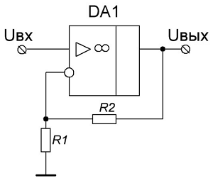
Schematic diagram of a non-inverting amplifier.
This circuit is one of the standard circuits for switching on operational amplifiers and contains the op-amp DA1, the bias resistor R1 and the feedback resistor R2. The operational amplifier in this circuit is covered by serial voltage feedback, the gain of the feedback circuit will be
In the simplest case, we will connect the circuit as follows. Then the input voltage will be equal to one tenth of the output. When we input a voltage of 0.5V at the input, the op-amp will increase the output voltage until the input voltage reaches the same level.
But this requires the output to be ten times the input voltage! Thus, the amplifier "forces" 10 times the voltage. We simply calculate the gain in the return circuit using the formula. An op-amp can also be connected so that the amplified signal has an inverted value. Against the previous connection, it is enough to replace the ground and the signal input.
Then the input impedance of the non-inverting amplifier will be
R BX.OU - input impedance of the OS with an open OS circuit,
TO OU - gain coefficient of the op-amp with an open OS circuit.
The output impedance of a non-inverting amplifier can be calculated from the following expression
Since there is zero voltage present at the input, the output must always have the opposite voltage to bias it. We will calculate the wiring inversion gain as follows. Positive feedback with negative feedback resistors as an integration article. The circuit alternately discharges and charges the capacitor. As an output, we can use rectangular and triangular waveforms. The voltages over time are on the graph.
The following 4 amplifier amps have 3 outputs that generate triangle, square and sine waveform with selectable frequency. The red part is a voltage divider, giving the op amps half the supply voltage as the center against which they amplify the AC signal. The yellow part is an oscillator in which a square and triangle signal is formed in nature. In the purple part of the triangular signal, we keep the amplitude but amplify the current so that possible sampling does not interfere with the frequency of the oscillator. The green section uses the diode's voltage drop to keep the edges of the triangle's steep edge for small deflections and attenuate the signal for large deflections. The blue part is a classic amplifier. This triangle signals a sinusoidal signal! . A useful connection will occur when we connect the output to the input only, and the signal is injected into the input.
R OUTPUT OU - output impedance of the OU with an open OS circuit.
Non-inverting amplifier gain

This type of amplifier has some level of input offset voltage UCM, so this circuit can be applied where the level of input offset voltage does not have a significant effect. The bias voltage level at the input will be
Although the circuit will not be amplified, it will allow current to be drawn at the output without the need for an input stream to flow. Thus, we can measure the voltage even in cases where the behavior of the circuit and the minimum current consumption may change. When we replace the feedback resistor with a capacitor, the output of the amplifier will be the integral of the input signal. In other words, the input-output ratio will be the same as the ratio of the speed of movement.
Operational amplifiers for everyone. . An operational amplifier is used to implement electronic integrated circuits, such as adding or subtracting voltages and currents. In real systems, the input impedance is very high, on the order of megaohms, and the voltage gain is on the order of tens of decibels. Due to the high input impedance, the operational amplifier does not load the signal source. Since it has a high voltage amplitude, the linear range is small, so systems of this type are designed to work with external feedback, usually negative feedback.
![]()
An example of calculating a non-inverting amplifier
We calculate a non-inverting amplifier, which should provide a gain of K = 10. As an op-amp, we use K157UD2, which has the following parameters: gain (at a frequency of 1 kHz) K = 1800 (65 dB), input impedance R BX.OU = 500 kOhm, output resistance R OUT.OU = 300 Ω, bias voltage U CM = 10 mV, input current I IN ≤ 500 nA. The input signal has a level U IN = 40 mV.
Non-inverting adder
Continuing the topic of non-inverting amplifiers, I will talk about a non-inverting adder that performs the function of adding input signals and finds its application as linear signal mixers (mixers), for example, when signals from several sources need to be combined and fed to the input of a power amplifier. The circuit of the non-inverting adder is shown below.
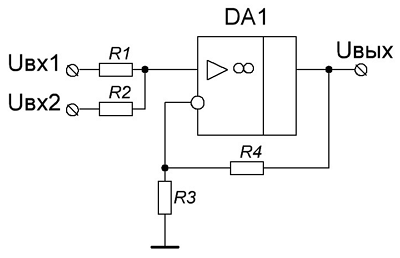
This circuit is a two-input non-inverting amplifier and consists of op-amp DA1, current-limiting input resistors R1 and R2, bias resistor R3, and feedback resistor R4.
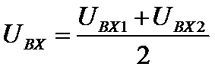
For this circuit, the basic relations correspond to the circuit of a simple non-inverting amplifier, taking into account the fact that the input voltage in the circuit corresponds to the average voltage of the input terminals
And the resistance of the resistors must meet the following condition
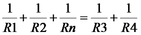
The gains for different channels are determined by the following expression
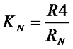
R N is the resistance of the input resistor,
K N is the gain of the corresponding amplification channel.
The main disadvantage of the non-inverting adder circuit is the lack of a zero potential point, so the gain on the various inputs is not independent. This disadvantage manifests itself in cases where the internal resistance of the input voltage sources or only one of them is known approximately or changes during operation.
Theory is good, but theory without practice is just shaking the air.
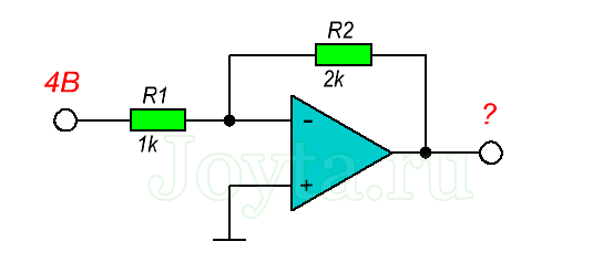
An inverting amplifier is one of the simplest and most commonly used analog circuits. With just two resistors, we can set the gain we need. Nothing prevents us from making the coefficient less than 1, thereby weakening the input signal.
Often, another R3 is added to the circuit, the resistance of which is equal to the sum of R1 and R2.
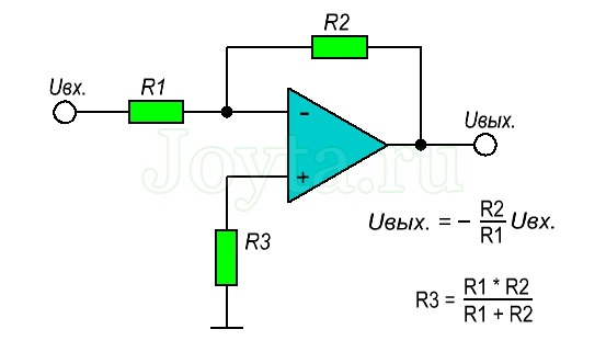
To understand how an inverting amplifier works, let's simulate a simple circuit. We have a voltage of 4V at the input, the resistance of the resistors is R1 \u003d 1k and R2 \u003d 2k. One could, of course, substitute all this into the formula and immediately calculate the result, but let's see how exactly this scheme works.
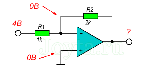
Let's start with a reminder of the basic principles of operation of an operational amplifier:
Rule No. 1 - the operational amplifier exerts its output on the input through the NOS (negative feedback), as a result of which the voltages at both inputs, both inverting (-) and non-inverting (+), are equalized.
Please note that the non-inverting input (+) is connected to ground, that is, the voltage on it is 0V. In accordance with rule #1, the inverting input (-) should also be 0V.
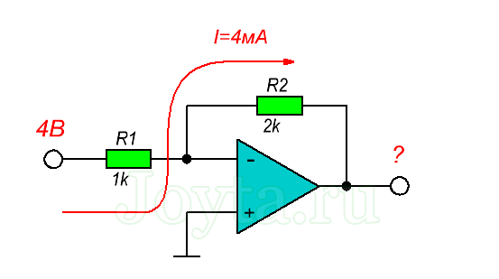
So, we know the voltage at the terminals of the resistor R1 and its resistance 1k. Thus, with the help we can perform the calculation, and calculate how much current flows through the resistor R1:
IR1 \u003d UR1 / R1 \u003d (4V-0V) / 1k \u003d 4mA.
Rule #2 - Amplifier Inputs Don't Draw Current
Thus, the current flowing through R1 flows further through R2!
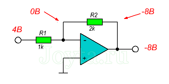
Again, we use Ohm's law and calculate what voltage drop occurs across the resistor R2. We know its resistance and we know what current through it, therefore:
UR2 = IR2R2 = 4mA *2k = 8V.
It turns out that we have 8V at the output? Not certainly in that way. Let me remind you that this is an inverting amplifier, that is, if we apply a positive voltage to the input, and remove the negative voltage at the output. How does it happen?
This is due to the fact that the feedback is set at the inverting input (-), and to equalize the voltages at the input, the amplifier reduces the potential at the output. Connections of resistors can be considered as simple, therefore, in order for the potential at the point of their connection to be equal to zero, the output must be minus 8 volts: Uout. = -(R2/R1)*Uin.
There is another catch associated with the 3rd rule:
Rule number 3 - the voltages at the inputs and outputs must be in the range between the positive and negative supply voltage of the op-amp.
That is, you need to check that the voltages calculated by us can actually be obtained through the amplifier. Often beginners think that the amplifier works as a source of free energy and generates voltage from nothing. But we must remember that the amplifier also needs power to work.
Classic amplifiers operate on voltages of -15V and +15V. In such a situation, our -8V, which we calculated, is the real voltage, since it is in this range.
However, modern amplifiers often operate at or below 5V. In such a situation, there is no chance that the amplifier will give us minus 8V at the output. Therefore, when designing circuits, always remember that theoretical calculations must always be supported by reality and physical capabilities.
It should be noted that the inverting amplifier has one drawback. We already know that it does not load the signal source, since the amplifier inputs have a very high resistance, and draw so little current that in most cases it can be ignored (rule # 2).
The inverting amplifier has an input impedance equal to the resistance of the resistor R1, in practice it ranges from 1k ... 1M. For comparison, an amplifier with field-effect transistor inputs has a resistance of the order of hundreds of megaohms and even gigaohms! Therefore, it may sometimes be advisable to install a voltage follower in front of the amplifier.