Star news


Transistors KT3102. Transistor KT3102: parameters and analogues, pinout
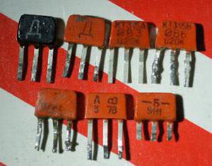
One of the most famous transistors is KT315, an analogue of which did not soon appear in the vastness of the Soviet Union, and which was the first mass-produced Soviet transistor. It is so universal that it continues to be used to this day (albeit quite limitedly and mostly by radio amateurs). The prerequisite for this was their versatility, long service life and extensive experience in creating something with their help (which can be found in special sources).
Development
Soviet engineers came up with the idea of mass production back in 1966. The transistor was developed in 1967 by the Fryazino Semiconductor Plant in its research and design bureau. And in 1968, the first units came off.
How does it stand out among other transistors?
 First of all, we paid attention to its appearance and characteristics. The frequency bar was 250 MHz, which as of 1967 was very, very high. Also, the ease of production led to the production of a huge number of transistors. There was also something unique (at that time) in the issues of grounding the negative pole of the power supply.
The technology behind the transistor
 For production, planar technology was used (it was envisaged that all structures were created on one side, the conductivity of the material was the same as in collectors, so first, when used, the base region is formed, and then the emitter region is formed in it). The parameters that he obtained made him the best in the world (at the time of creation). It made it possible to replace many other parts in electronics, while being cheap. It got to the point that in the Soviet Union, stores for radio amateurs sold it by weight.
KT315 - domestic and foreign analogues
 But since the main topic of the article is not KT315 - analogues for this transistor, attention should already be paid to the main topic. So, here is a list of analogues:
- Bipolar transistor BC847B. A relatively expensive (3 rubles per 1 piece) low-power transistor with a significant gain. Compared to KT315, the foreign analogue is quite expensive. But it has the advantage that when soldering and re-soldering it does not fail so quickly (which is not least due to its enlarged and reinforced design). Maximum power dissipation - 0.25. Up to 50 Volts can be supplied to the collector-base direction. To the collector-emitter - up to 45 Volts. The maximum voltage for the emitter-base direction is 6 Volts. The collector junction has a capacity of 8. The maximum junction temperature is 150 degrees. Statistical current transfer coefficient - 200.
- Bipolar transistor 2SC634. This imported analogue of KT315 is quite balanced in terms of characteristics and price. The maximum power dissipation value is 0.18. The maximum permissible voltage on the collector-base and collector-emitter is 40 Volts. Emitter-base - only 6 Volts. The collector junction capacity is 8. The maximum junction temperature is 125 degrees. Static current transfer coefficient is 90.
- Bipolar transistor KT3102. To say that for KT315 it is a domestic analogue would be incorrect, because historically it so happened that such parts were manufactured of one type, which meets all the necessary requests and can perform the functions assigned to it. The fact is that simply KT3102 does not exist; another letter must follow. To avoid conflicts, values will be specified for the entire group. You can get more detailed information by looking at each transistor. The domestic development is an improved KT315. Analog in this case is not an entirely appropriate word, but rather an improved mechanism. The maximum power dissipation of KT3102 is 0.25. A maximum voltage of 20-50 Volts can be supplied to the base collector. The maximum voltage that can be supplied to the collector-emitter is also 20-50 Volts. The maximum voltage to the emitter-base is 5 Volts. The capacitance of the collector junction is 6. The maximum junction temperature is 150 degrees. The static current transfer coefficient is 100.
- Bipolar transistor 2SC641. Maximum power dissipation - 0.1. The voltage in the collector-base direction should not exceed 40 Volts. The maximum voltage in the collector-emitter direction should not be more than 15 Volts. For the emitter-base direction, this value should not exceed 5 Volts. The collector junction capacity is 6 units. The maximum transition temperature is 125 degrees. The static current transfer coefficient is 35.
Where are they used?
KT315, analogues (foreign and domestic) have been and are now used by radio amateurs to create amplifiers for high, medium and low frequencies. They can also be used in generators, signal converters and logic circuits. If you use your brain, you can find other uses, but this is the main purpose for the KT315. The parameters of the analog (any) are slightly different. But the main thing is that these are bipolar transistors, and their power is important solely for the power of the circuits that will be assembled.
Conclusion
 The article examined the prototype (KT315) and its analogs with a description of the possibilities of their use. We hope that the information provided here will be useful to you. It is also necessary to recall that transistors are rather fragile elements, which also often burn out. Therefore, when working with them, and with other electrical parts, follow safety precautions.
A transistor is a semiconductor element of an electrical circuit controlled by an input signal. The signal can be used as a conventional electric current, but also, for example, light in the operation of a phototransistor.
Transistor KT3102 is the most popular Soviet bipolar transistor, which was and is still used today in circuits of various signal amplifiers: operational amplifiers, differential and ULF (low frequency amplifier). KT3102, due to the small thickness of the base, amplified the current signal thousands of times. It is made of silicon, most often by epitaxy (growth of new semiconductor layers on a silicon substrate).
The KT3102 transistor was initially most often manufactured in a metal cylindrical case, familiar to many Soviet transistors. At the moment, it is manufactured in a plastic case. It is a complementary pair for KT3107.
The operating principle of the device is to control the current by changing the voltage. In order for the element to start working, voltage must be applied to it. Then the device will open. By changing the base voltage, we control the entire element.
There is quite a large number various options of this device, differing from each other in certain indicators. To consider all variants of the device, we introduce the following parameters of KT3102:
The above characteristics of KT3102 are the same for all models of the device. That is, with any marking of the device, you must take into account the above values. The metrics described below will vary depending on the item type. Subsequently we will present a brief summary of the parameters for each type.
- U KB – maximum potential difference of the collector-base system.
- U CE – maximum potential difference of the collector-emitter system.
- H 21e – gain when connected to a common emitter.
- I KB – reverse collector current.
- KSh – noise factor.
For convenience, all indicators will be presented in a table. The letter M and its absence in the designation of a pair of transistors (for example, KT3102A and KT3102AM) means the type of housing. With the letter M - plastic case. Without it - metal. The indicators do not depend on the type of case. The table will also show foreign analogues of KT3102.
| Type | U KB and U CE, V | H 21 E | I KB, MkA | K Sh, db | Analogue KT3102 |
| KT3102A(AM) | 50 | 100-250 | 0,05 | 10 | 2 N 4123 |
| KT3102B(BM) | 50 | 200-500 | 0,05 | 10 | 2N2483 |
| KT3102V(VM) | 30 | 200-500 | 0,15 | 10 | 2SC828 |
| KT3102G(GM) | 20 | 400-1000 | 0,15 | 10 | BC546C |
| KT3102D(DM) | 30 | 200-500 | 0,15 | 4 | BC547B |
| KT3102E(EM) | 20 | 400-1000 | 0,15 | 4 | BC547C |
| KT3102Zh(ZhM) | 50 | 100-250 | 0,05 | — | — |
| KT3102I(IM) | 50 | 200-500 | 0,05 | — | — |
| KT3102K(KM) | 20 and 30 | 200-500 | 0,15 | — | — |
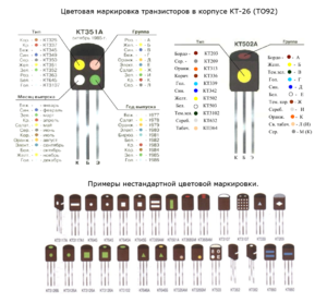
Marking and pinout
This device has the structure n - p - n. The terminals of the element from left to right, when the front part of the transistor is facing us (flat side with markings), have the following order - “collector-base-emitter”. You need to know the pinout of the KT3102 and take it into account when soldering the device. A soldering error can damage the entire transistor.
Transistor markings are used to distinguish one type of device from another. For example, the differences between type A and B. In the case of KT3102, The marking has the following structure:
- The green circle on the front side indicates the type of transistor. In our case - KT3102.
- The circle on top indicates the letter of the device (A, B, C, etc.). The following designations apply:
A – red or burgundy. B – yellow. B – green. G – blue. D – blue. E – white. F – dark brown.
On some devices, instead of color designations, the markings are written in words. For example, 3102 EM. Such designations are more convenient than colored ones.
Knowing the transistor markings will allow you to correctly select the right element according to the required parameters.
Foreign analogs of KT3102
 To replace KT 3102 there are a very large number of foreign analogues of KT 3102. The analogue can be absolutely identical to the original, for example, KT3102 can be safely replaced with 2 SA 2785. This replacement of KT 3102 will have absolutely no effect on the operation of a particular circuit, since the transistors have the same performance. There are also non-identical analogs that differ slightly in performance, but their use is still possible in some cases.
Some foreign analogues of KT3102 were listed in the table. Also, this device can be replaced by domestic analogues KT611 and KT660 or by foreign analogues such as BC547 and BC548.
List and quantity of precious metals that can be extracted from the KT3102BM transistor.
Information from manufacturers' directories. A directory of the content of precious metals (gold, silver, platinum and PGM) in a transistor, indicating its weight, which are used (or were used) in production in radio engineering.
Transistor, semiconductor triode- a radio-electronic component made of semiconductor material, usually with three terminals, allowing an input signal to control a current in electrical circuit. Typically used to amplify, generate and convert electrical signals. In general, a transistor is any device that simulates the main property of a transistor - the change in signal between two different states when the signal at the control electrode changes.
In field-effect and bipolar transistors, the current in the output circuit is controlled by changing the input voltage or current. A small change in input quantities can lead to a significantly larger change in output voltage and current. This amplifying property of transistors is used in analog technology (analog TV, radio, communications, etc.). Currently, analog technology is dominated by bipolar transistors (BT) (the international term is BJT, bipolar junction transistor). Another important branch of electronics is digital technology (logic, memory, processors, computers, digital communications, etc.), where, on the contrary, bipolar transistors are almost completely replaced by field-effect ones.
Now let's talk about field effect transistors. What can you assume from their name alone? Firstly, since they are transistors, they can be used to somehow control the output current. Secondly, they are supposed to have three contacts. And thirdly, their work is based on the p-n junction. What will official sources tell us about this?
Field-effect transistors are active semiconductor devices, usually with three terminals, in which the output current is controlled using an electric field.
The definition not only confirmed our assumptions, but also demonstrated a feature of field-effect transistors - the output current is controlled by changing the applied electric field, i.e. voltage. But at bipolar transistors, as we remember, the output current is controlled by the input base current.
Another fact about field-effect transistors can be found by paying attention to their other name - unipolar. This means that only one type of charge carrier (either electrons or holes) is involved in the process of current flow.
The three contacts of field-effect transistors are called the source (the source of current carriers), the gate (the control electrode) and the drain (the electrode where the carriers flow). The structure seems simple and very similar to the design of a bipolar transistor. But it can be implemented in at least two ways. Therefore, field-effect transistors are distinguished with control p-n junction and with an insulated shutter.
Transistor circuit and transistor switching circuit.
Any amplifier, regardless of frequency, contains from one to several amplification stages. In order to have an idea of the circuit design of transistor amplifiers, let us consider their circuit diagrams in more detail.
Transistor stages, depending on the options for connecting transistors, are divided into:
1 Cascade with a common emitter (the diagram shows a cascade with a fixed base current - this is one of the types of transistor bias).
2 Cascade with common collector
3 Cascade with a common base
Transistor parameters
UCBO - maximum permissible collector-base voltage;
UKBO and - maximum permissible pulse voltage collector - base;
UCEO - maximum permissible collector-emitter voltage;
UCEO and - maximum permissible pulse voltage collector-emitter;
UKEN - collector-emitter saturation voltage;
USI max - maximum permissible drain-source voltage;
USIO - drain-source voltage when the gate is broken;
UZ max - maximum permissible gate-source voltage;
UZI ots - Transistor cut-off voltage at which the drain current reaches a specified low value (for field-effect transistors with a p-n junction and with an insulated gate);
UZI pore - Threshold voltage of the transistor between the gate and drain, at which the drain current reaches a specified low value (for field-effect transistors with an insulated gate and n-channel);
IK max - maximum permissible D.C. collector;
IK max and is the maximum permissible pulse current of the collector;
IC max - maximum permissible constant drain current;
IC start - initial drain current;
IC rest - residual drain current;
IKBO - reverse collector current;
RK max - maximum permissible constant power dissipation of the collector without heat sink;
RK max t - maximum permissible constant power dissipation of the collector with a heat sink;
RSI max - maximum permissible constant power dissipation drain - source;
H21E - static current transfer coefficient of a bipolar transistor in a circuit with a common emitter;
RSI open - resistance drain - source in open state;
S is the slope of the characteristic;
fGR. — cut-off frequency of the current transfer coefficient in a circuit with a common emitter;
KS - noise figure of a bipolar (field-effect) transistor;
Transistor connection circuits
To be included in the circuit, the transistor must have four terminals - two input and two output. But transistors of all varieties have only three terminals. To turn on a three-terminal device, it is necessary to combine one of the terminals, and since there can only be three such combinations, there are three basic circuits for connecting a transistor:
Bipolar transistor connection circuits
with a common emitter (CE) - provides amplification in both current and voltage - the most commonly used circuit;
with a common collector (OC) - provides amplification only by current - used to match high-impedance signal sources with low-impedance load resistances;
with a common base (CB) - amplification only by voltage; due to its shortcomings, it is rarely used in single-transistor amplification stages (mainly in microwave amplifiers), usually in composite circuits (for example, cascode).
Field-effect transistor connection circuits
Field-effect transistors, both with p-n junction (channel) and MOS (MDS), have the following connection circuits:
with a common source (CS) - an analogue of a OE bipolar transistor;
with a common drain (OC) - an analogue of an OK bipolar transistor;
with a common gate (OG) - an analogue of the OB of a bipolar transistor.
Open collector (drain) circuits
“Open collector (drain)” is the connection of a transistor according to a circuit with a common emitter (source) as part of an electronic module or microcircuit, when the collector (drain) terminal is not connected to other elements of the module (microcircuit), but is directly brought out (to the module connector or microcircuit output). The choice of transistor load and collector (drain) current is left to the developer of the final circuit, which includes a module or microcircuit. In particular, the load of such a transistor can be connected to a power source with a higher or lower voltage than the supply voltage of the module/chip. This approach significantly expands the scope of applicability of a module or microcircuit due to a slight complication of the final circuit. Transistors with an open collector (drain) are used in TTL logic elements, microcircuits with powerful key output stages, level converters, bus shapers (drivers), etc.
Less commonly used is reverse connection - with an open emitter (source). It also allows you to select the transistor load after the main circuit has been manufactured, supplying the emitter/drain voltage with a polarity opposite to the main circuit supply voltage (for example, negative voltage for circuits with bipolar n-p-n transistors or N-channel field), etc.
Transistor marking - Color and code marking of transistors.
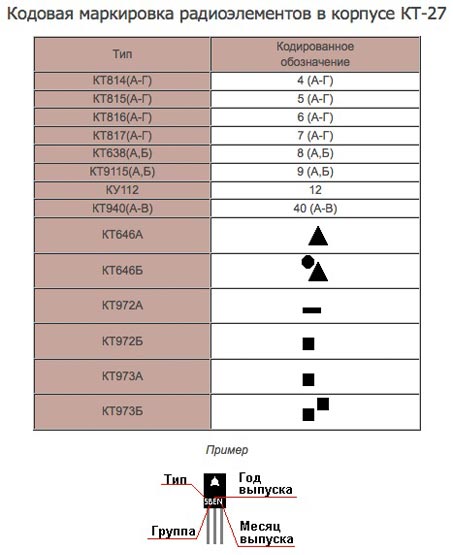
Code marking of the date of manufacture of devices
Year Coded designation
1983 R
1984S
1985 T
1986U
1987 V
1988W
1989 X
1990A
1991 B
1992 C
1993D
1994E
1995 F
1996H
1997 J
1998 K
1999L
N2000
Month Coded designation
January 1
February 2
March 3
April 4
May 5
June 6
July 7
August 8
September 9
October 0
November N
December D
Group color coding
Group Colored dot on top
A Dark red
B Yellow
B Dark green
G Blue
D Blue
E White
F Dark brown
And Silver
K Orange
L Light tobacco
M Gray
Transistor pinout
When selecting analogue parts according to diagrams, the question of their correct installation on the printed circuit board always arises. Pinout of transistors. Now I want to describe and lay out on one page the pinouts (pinouts) of all domestic transistors, so that you are not misled by the question of the location of the transistor legs.
Transistors reference book - transistor housings

transistors directory - transistor housings
Working Principle of Transistor
Currently, two types of transistors are used - bipolar and field-effect. Bipolar transistors appeared first and became most widespread. Therefore, they are usually simply called transistors. Field-effect transistors appeared later and are still used less frequently than bipolar ones.
Bipolar transistors are called because the electric current in them is formed by electric charges of positive and negative polarity. Positive charge carriers are usually called holes, negative charges are carried by electrons. A bipolar transistor uses a crystal made of germanium or silicon - the main semiconductor materials used to make transistors and diodes. That's why some transistors are called silicon, others - germanium. Both types of bipolar transistors have their own characteristics, which are usually taken into account when designing devices.
buy transistors, transistor price
If you have more information about the KT3102BM transformer, please let us know, we will post it on the website for free.
Photo transistor KT3102BM:

Characteristics of transistor KT3102BM:
Buy or sell as well as prices for the KT3102BM transistor (buy transistors, transistor price):
Leave a review or a free ad to buy or sell