Star News


Schemes of operation of transistors with explanations. What is the difference between NPN and PNP transistors
A transistor, as a semiconductor device with three electrodes (emitter, base, collector), can be turned on in three main ways (Fig. 3.1 - 3.6). As you know, the input signal goes to the amplifier through two wires; the output signal is also diverted via two wires. Consequently, for a three-electrode amplifying device, when an input signal is applied and an output signal is removed via two wires, one of the electrodes will certainly be common. According to which of the electrodes in the transistor switching circuit will be common, there are three main switching circuits: with a common emitter (OE), a common collector (OK) and a common base (OB).
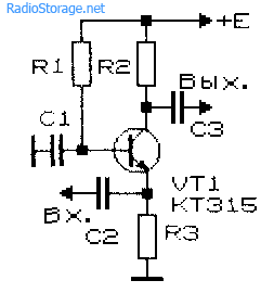
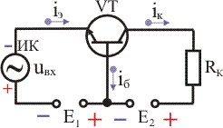
Rice. 3.1. Common emitter (CE) circuit

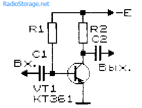
Rice. 3.2. Common collector circuit (OK)
Practical options for switching transistors p-p-p structures and p-n-p are shown in fig. 3.1 - 3.6. As follows from a comparison of the figures, these circuits are identical and differ only in the polarity of the applied voltage.
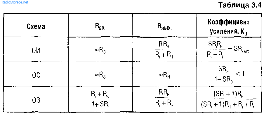
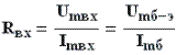
To determine the input (RBX.) and output (RBbix.) resistance of each of the switching circuits, as well as the current gain (K,), voltage (Ki) and power (KR \u003d K | XKi), the calculated and experimental values \u200b\u200band formulas are given in tables 3.1 and 3.2.
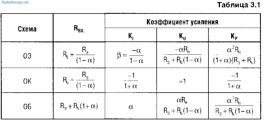
![]()
The table with formulas is given for approximate calculations, and for the initial, primary assessment and comparison of the properties of the main transistor switching circuits, the second table with numerical estimates is intended.
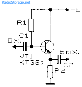
Rice. 3.3. Scheme with a common base (OB)
The designations in the table are as follows: RH is the load resistance; R3 is the emitter resistance or the ratio of the change in voltage at the emitter junction to the change in the emitter current in the short circuit mode in the output circuit for alternating current; RB is the base resistance or the ratio of the change in voltage between the emitter and the base to the change in collector current in the idle mode of the input circuit for alternating current; a is the current gain for a circuit with a common base; p is the current gain for a circuit with a common emitter.
Rice. 3.4. Common emitter (CE) circuit
Rice. 3.5. Common collector circuit (OK)
Rice. 3.6. Scheme with a common base (OB)
Most often, in practical circuits, the mode of switching on a transistor with a common emitter is used (as it has the highest power gain).
Emitter followers (common-collector circuits) are used to match the high output impedance of a signal source with a low input load impedance. To build high-frequency amplifiers (having a low input impedance), circuits with a common base are used.
Depending on the presence, polarity and magnitude of potentials on the electrodes of transistors, several modes of operation are distinguished. Saturation - the transistor is open, the voltage at the K-E junction is minimal, the current through the junctions is maximum. Cutoff - the transistor is closed, the voltage at the K-E junction is maximum, the current through the junctions is minimal. Active - intermediate between saturation and cutoff modes. Inverse - characterized by the supply of reverse (inverse) polarity of the operating voltage to the electrodes of the transistor.
In switching circuits that have only two states: on (the resistance of the key element is close to zero) and off (the resistance of the key element tends to infinity), saturation and cutoff modes are used. Active mode is widely used to amplify signals. The inverse mode is used quite rarely, since it is not possible to improve the performance of the circuit with this inclusion of the transistor.
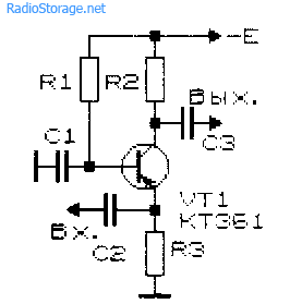
In order to initially estimate the values of the RC elements that make up the circuits without calculations (Fig. 3.1, 3.2, 3.4, 3.5), you can take the resistance value in the collector (emitter) circuit to be several kOhm, and the resistance value in the base circuit to 30 ...50 times large. In this case, the voltage at the collector (emitter) should be equal to half the supply voltage. For a circuit with a common base (Fig. 3.3, 3.6), the resistance value R3 usually does not exceed 0.1 ... 1 kOhm, the resistance value R2 is several kOhm.
The values of the reactive resistances of the capacitors C1 - SZ for the lowest frequencies that need to be strengthened should be approximately an order of magnitude lower than the active resistances R1 - R3 connected to them (Fig. 3.1 - 3.6). In principle, the values of these capacitances could be chosen with a significant margin, but in this case, the dimensions of the transition capacitors, their cost, leakage currents, the duration of transients, etc. increase.
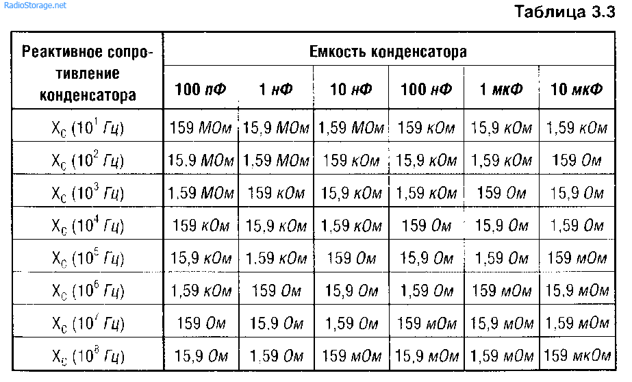
As an example, let's use Table 3.3 to quickly determine the reactance of capacitors for several frequencies.
Recall that the reactance of the capacitor Xc, Ohm, can be calculated by the formula:
For direct current, the reactance of capacitors tends to infinity. Therefore, for DC amplifiers (the lower gain cut-off frequency is zero), transient capacitors are not required, and special measures must be taken to separate the stages. Capacitors in DC circuits are tantamount to an open circuit. Therefore, when constructing DC amplifier circuits, circuits with direct connections between stages are used. Of course, in this case it is necessary to match the levels of interstage voltages.
When amplifying alternating current in the load circuit of amplifying stages, inductive elements are often used. Note that the reactance of inductors increases with increasing frequency. Accordingly, with a change in load resistance from frequency, the gain of such a cascade also increases.
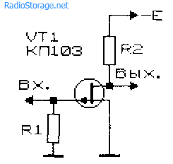
In addition to bipolar transistors, more modern elements, field-effect transistors, have become widespread (Fig. 3.7 - 3.9).
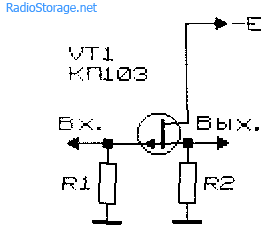
Rice. 3.7. Common Source (OI) Circuit
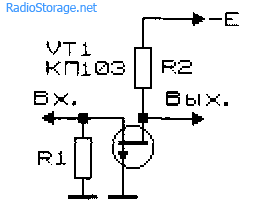
Rice. 3.8. Scheme with a common drain (OS)
By analogy with the circuits for switching on bipolar transistors, field transistors are switched on with a common source, a common drain, and with a common gate.
Rice. 3.9. Common gate circuit (03)
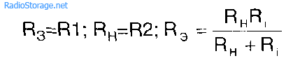
The main calculated ratios for these circuits for switching on field-effect transistors are given in Table 3.4, where S is the slope of the field-effect transistor characteristic, mA / V; R, is the internal resistance of the transistor.
Approximately the value of R1 (Fig. 3.7 - 3.9) can be from several ohms to units of MΩ R2 - several kΩ. Note that, as for bipolar transistors, field-effect transistors also allow operation with cutoff, with saturation; active and inverted modes.
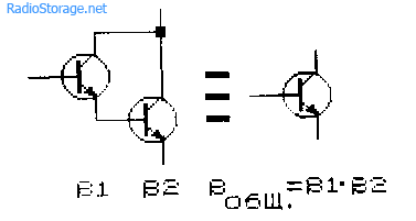
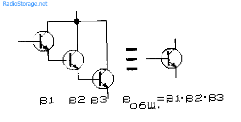
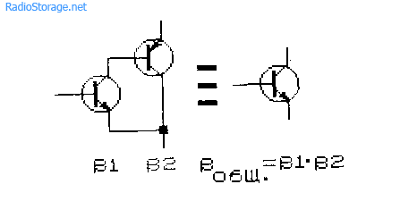
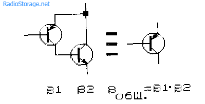
To increase the current transfer coefficient bipolar transistor use "composite" transistors, switched on according to the Darlington circuit (Fig. 3.10 - 3.13). Their overall gain is somewhat different from the product of the gains of each of the transistors. At the same time, the temperature stability of the circuit deteriorates.
Literature: Shustov M.A. Practical Circuitry (Book 1), 2003
There are two main types of transistors - bipolar and field. Bipolar transistors are made from doped materials and can be of two types - NPN and PNP. The transistor has three terminals, known as emitter (E), base (B), and collector (C). The figure below shows an NPN transistor where, in the main operating modes (active, saturation, cutoff), the collector has a positive potential, the emitter is negative, and the base is used to control the state of the transistor.
An NPN transistor has one P region sandwiched between two N regions:
 |
The junctions between the N and P regions are similar to the junctions in diodes, and they can also be forward and reverse biased. p-n junction. These devices can operate in different modes depending on the type of bias:
- Cutoff: This mode also works when switching. No current flows between the emitter and the collector, practically an “open circuit”, that is, “the contact is open”.
- Active mode: the transistor works in amplifier circuits. In this mode, its characteristic is almost linear. A current flows between the emitter and the collector, the value of which depends on the value of the bias (control) voltage between the emitter and the base.
- Saturation: works when switched. There is practically a "short circuit" between the emitter and the collector, that is, "the contact is closed".
- Inverse active mode: As in active mode, the transistor current is proportional to the base current, but flows in the opposite direction. Used very rarely.
In an NPN transistor, a positive voltage is applied to the collector to create current from the collector to the emitter. In a PNP transistor, a positive voltage is applied to the emitter to create current from the emitter to the collector. In NPN current flows from collector (K) to emitter (E):
It is clear that the directions of current and voltage polarity in PNP and NPN are always opposite to each other. NPN transistors require positive power to ground, while PNP transistors require negative power.
PNP and NPN work almost the same, but their modes differ due to polarities. For example, to bring NPN into saturation mode, U B must be higher than U K and U E. The following is short description operating modes depending on their voltage:
 |
The basic principle of any bipolar transistor is to control the base current to regulate the flow of current between the emitter and collector. The principle of operation of NPN and PNP transistors is the same. The only difference is the polarity of the voltages applied to their N-P-N and P-N-P junctions, that is, to the emitter-base-collector.
There are three main switching circuits for transistors. In this case, one of the transistor electrodes is a common entry and exit point of the cascade. It must be remembered that the input (output) is understood as the points between which the input (output) alternating voltage acts. The main switching circuits are called circuits with a common emitter (OE), a common base (OB) and a common collector (OK).
Circuit with a common emitter (CE). Such a circuit is shown in Figure 1. All books say that this circuit is the most common, because it gives the greatest power gain.
Rice. 1 - Scheme for switching on a transistor with a common emitter
The amplifying properties of a transistor are characterized by one of its main parameters - the static current transfer coefficient of the base or the static current gain?. Since it should characterize only the transistor itself, it is determined in no-load mode (R k \u003d 0). Numerically it is equal to:
at U k-e = const
This coefficient can be equal to tens or hundreds, but the real coefficient k i is always less than ?, because when the load is turned on, the collector current decreases.
The voltage gain of the cascade k u is equal to the ratio of the amplitude or effective values output and input AC voltage. The input is the alternating voltage u b-e, and the output is the alternating voltage across the resistor, or equivalently, the collector-emitter voltage. The base-emitter voltage does not exceed tenths of a volt, and the output reaches units and tens of volts (with sufficient load resistance and source voltage E 2). It follows from this that the power gain of the cascade is equal to hundreds, thousands, and sometimes tens of thousands.
An important characteristic is the input resistance R in, which is determined by Ohm's law:
and usually ranges from hundreds of ohms to units of kilo-ohms. The input resistance of the transistor when switched on according to the OE circuit, as can be seen, is relatively small, which is a significant drawback. It is also important to note that the stage according to the OE circuit reverses the phase of the voltage by 180 °
The advantages of the OE circuit include the convenience of powering it from a single source, since the base and collector are supplied with supply voltages of the same sign. The disadvantages include the worst frequency and temperature properties (for example, in comparison with the OB circuit). As the frequency increases, the gain in the OE circuit decreases. In addition, the cascade according to the OE scheme introduces significant distortions during amplification.
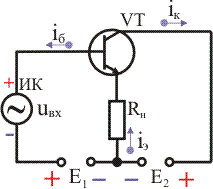
Scheme with a common base (OB). The OB scheme is shown in Figure 2.
Rice. 2 - Scheme for switching on a transistor with a common base
Such a switching circuit does not provide significant amplification, but has good frequency and temperature properties. It is not used as often as the OE scheme.
The current gain of the OB circuit is always slightly less than one:
since the collector current is always only slightly less than the emitter current.
The static current transfer coefficient for the OB circuit is indicated? and is defined:
for u k-b = const
This coefficient is always less than 1 and the closer it is to 1, the better the transistor. The voltage gain is the same as in the OE circuit. The input impedance of the OB circuit is ten times lower than in the OE circuit.
For the OB circuit, there is no phase shift between the input and output voltage, that is, the phase of the voltage does not reverse during amplification. In addition, when amplified, the OB circuit introduces much less distortion than the OE circuit.
Scheme with a common collector (OK). The switching circuit with a common collector is shown in Figure 3. Such a circuit is more often called an emitter follower.
Rice. 3 - Scheme for switching on a transistor with a common collector
The peculiarity of this circuit is that the input voltage is completely transferred back to the input, i.e., negative feedback is very strong. The current gain is almost the same as in the OE circuit. The voltage gain approaches unity, but is always less than it. As a result, the power gain is approximately equal to k i , i.e., several tens.
In the OK circuit, there is no phase shift between the input and output voltage. Since the voltage gain is close to unity, the output voltage coincides in phase and amplitude with the input, i.e. repeats it. That is why such a circuit is called an emitter follower. Emitter - because the output voltage is removed from the emitter relative to the common wire.
The input resistance of the OK circuit is quite high (tens of kilo-ohms), and the output resistance is relatively small. This is an important advantage of the scheme.
The OE circuit has the highest power gain, so it remains the most common solution for high-frequency amplifiers, GPS, GSM, WiFi systems. Currently, it is usually used in the form of ready-made integrated circuits (MAXIM, VISHAY, RF Micro Devices), but without knowing the basics of its operation, it is almost impossible to obtain the parameters given in the description of the microcircuit. That is why, when hiring and searching for employees, the main requirement is the knowledge of the principles of operation of amplifiers with OE.
An amplifier, whatever it is, (audio amplifier, tube amplifier or radio frequency amplifier) is a four-terminal circuit, in which two terminals are input and two terminals are output. The block diagram of the amplifier is shown in Figure 1.
Figure 1 Structural diagram of switching on the amplifier
The main amplifying element - the transistor has only three outputs, so one of the outputs of the transistor must be used simultaneously to connect the signal source (as an input terminal) and connect the load (as an output terminal). A common-emitter circuit is an amplifier where the emitter of a transistor is used both to connect the input signal and to connect the load. A functional diagram of an amplifier with a transistor connected according to a common emitter circuit is shown in Figure 2.
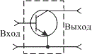
Figure 2 Functional diagram of switching on a transistor with a common emitter
In this diagram, the dotted line shows the boundaries of the amplifier shown in Figure 1. It does not show the power circuits of the transistor. At present, the common emitter circuit is practically not used in audio amplifiers, however, in television signal amplifier circuits, GSM amplifiers or other high-frequency amplifiers, it is widely used. Two power supplies can be used to power the transistor in a common-emitter circuit, but this requires two voltage regulators. This can be problematic in battery-powered equipment, so a single power supply is usually used. To power an amplifier with a common emitter, any of the circuits we have considered can be suitable:
- emitter stabilized circuit.
Consider an example of an amplifier circuit with a common emitter and emitter stabilization of the transistor operation mode. Figure 3 shows a schematic diagram of a cascade on a bipolar npn transistor, designed to amplify audio frequencies.
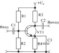
Figure 3 circuit diagram amplifying stage with a common emitter
Calculation of the elements of this scheme according to direct current can be seen in the article. Now we will be interested in the parameters of the amplifying stage, assembled according to the scheme with a common emitter. The most important characteristics of an amplifier stage are its input and output impedance and power gain. Basically, these characteristics are determined by the parameters of the transistor.
Common emitter input impedance
In a common emitter circuit, the input resistance of the transistor is R The input characteristic can be determined from its input characteristic. This characteristic coincides with the current-voltage characteristic p-n transition. An example of the input characteristic of a silicon transistor (voltage dependence U b from base current I b) is shown in Figure 4.
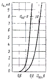
Figure 4 Silicon Transistor Input Characteristic
As can be seen from this figure, the input resistance of the transistor R VhOE depends on the base current I b0 and is determined by the following formula:
How to determine Δ U b0 and Δ I b0 in the vicinity of the operating point of the transistor in a circuit with a common emitter is shown in Figure 5.
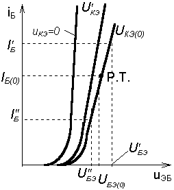
Figure 5 Determining the Input Resistance of a Common Emitter Circuit from the Input Characteristic of a Silicon Transistor
Determination of resistance by formula (1) is the most accurate way to determine the input resistance. However, when calculating an amplifier, we do not always have the transistors we will use on hand, so it would be nice to be able to calculate the input resistance in an analytical way. The current-voltage characteristic of the p-n junction is well approximated by an exponential function.
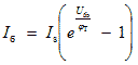 (2)
(2)
where I b - base current at the operating point;
U be is the base voltage at the operating point;
I s- reverse current emitter-base junction;
— temperature potential;
k is the Boltzmann constant;
q is the electron charge;
T is the temperature expressed in degrees Kelvin.
In this expression, the coefficient normalizing the exponent is the current I s , so the more precisely it is determined, the better will be the coincidence of the real and approximate input characteristics of the transistor. If one is neglected in expression (2), then the voltage at the base of the transistor can be calculated using the following formula:
From expression (1) it can be seen that the input resistance is the derivative of the voltage at the base of the transistor with respect to current. Let's differentiate expression (3), then the input impedance of the circuit with a common emitter can be determined by the following formula:
(4)However, the graph of the real input characteristic of a transistor connected according to a common emitter circuit differs from an exponential function. This is due to the fact that the ohmic resistance of the semiconductor in the base of the transistor is not equal to zero, therefore, at high base currents of the transistor in a circuit with a common emitter, its input resistance will tend to the ohmic resistance of the base r bb ".
The input current of the common-emitter circuit flows not only through the input resistance of the transistor, but also through all the resistors of the voltage generating circuits at the base of the transistor. Therefore, the input resistance of a common-emitter circuit is defined as the parallel connection of all these resistances. The common-emitter input current paths are shown in Figure 6.
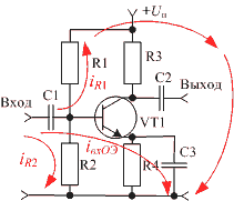
Figure 6 Current flow through the input circuits of a common-emitter circuit
It is much easier to analyze this circuit using the equivalent circuit of the input circuit, which shows only those circuits through which the input current flows from the signal source. The equivalent circuit of the input circuit of the common emitter circuit is shown in Figure 7.
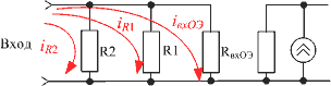
Figure 7 Common Emitter Input Circuit Equivalent Circuit
This circuit is built for medium frequencies using a transistor equivalent circuit. At medium frequencies, the input capacitance of the transistor has no effect, so we do not display it on the equivalent circuit. The resistance of the capacitor C3 at medium frequencies is close to zero, so there are no R4C3 elements in the circuit. Elements R out and h 21× i in do not affect the input circuit and are shown in the diagram to display the amplifying properties of the transistor.
And finally, we can write the formula for the input impedance of a common-emitter circuit:
(5)After manufacturing the amplifier, calculated according to the above methods, it is necessary to measure the input resistance of the circuit with a common emitter. To measure the input resistance, use the circuit for measuring the input resistance of the amplifier, shown in Figure 8. In this circuit, to measure the input resistance, a measuring alternating voltage generator and two high-frequency AC voltmeters are used (you can use one and make two measurements).
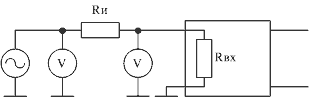
Figure 8 Scheme for measuring the input resistance of the amplifier stage
In case the resistance R and will be equal to the input impedance of the amplifier, the voltage that the AC voltmeter V2 will show will be half the voltage of V1. If there is no way to change the resistance R and when measuring the input impedance, the input impedance of the amplifier can be calculated using the following formula:
(6)Output impedance of a common-emitter circuit
The output resistance of a transistor depends on the design features of the transistor, the thickness of its base, and the bulk resistance of the collector. The output resistance of a common-emitter transistor can be determined from the output characteristics of the transistor. An example of the output characteristics of a transistor is shown in Figure 9.
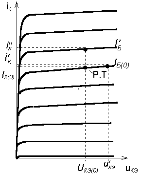
Figure 9 Silicon transistor output characteristics
Unfortunately, in the characteristics of modern transistors, output characteristics are usually not given. This is due to the fact that their output impedance is quite large and the output impedance of the transistor stage with a common emitter is determined by the load resistance. In the circuit shown in Figure 6, this is the resistance of the resistor R3.
Literature:
Together with the article "Common emitter circuit (common emitter cascade)" they read:
http://website/Sxemoteh/ShTrzKask/KollStab/
http://website/Sxemoteh/ShTrzKask/EmitStab/
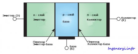
Bipolartransistor - three-electrode semiconductor device, one of the types transistor. The electrodes are connected to three consecutive layers of an interleaved type semiconductor. impurity conductivity. According to this method of alternation, n-p-n and p-n-p transistors ( n (negative) - electronic type of impurity conductivity, p (positive) - hole). In a bipolar transistor, unlike field effect transistor, two types of charges are used simultaneously, the carriers of which are electrons and holes (from the word "bi" - "two"). The schematic diagram of the transistor is shown in the second figure.
The electrode connected to the central layer is called base, the electrodes connected to the outer layers are called collector and emitter. On the the simplest circuit the differences between collector and emitter are not visible. In reality, the main difference between the collector is a larger area pn junction. In addition, a small base thickness is required for the transistor to work.
Device and principle of operation
Simplified cross-sectional diagram of an NPN bipolar transistor
The first transistors were made on the basis of Germany. Currently, they are mainly made from silicon and gallium arsenide. Gallium arsenide transistors are used in ultra-high-speed logic circuits and in high-frequency amplifier circuits.
A bipolar transistor is made up of three different alloyed semiconductor layers: emitter E, base B and collector C. Depending on the type of conduction of these zones, there are NPN(emitter − n-semiconductor, base − p- semiconductor, collector − n- semiconductor) and PNP transistors. Conductive non-rectifying contacts are connected to each of the zones. The base is located between the emitter and the collector and is lightly doped, therefore it has a large ohmic resistance. The total area of the base-emitter contact is much smaller than the area of the collector-base contact (this is done for two reasons - the large area of the collector-base junction increases the probability of capturing minor charge carriers from the base to the collector and, since in the operating mode the collector-base junction is usually switched on with reverse bias, which increases heat generation, promotes heat removal from the collector), therefore, a general bipolar transistor is an asymmetric device (it is not advisable to reverse the emitter and collector by changing the polarity of the connection and, as a result, obtain a bipolar transistor similar to the original - inverse connection).
In the active amplifying mode of operation, the transistor is turned on so that its emitter junction displaced in the forward direction (open), and the collector junction is biased in the opposite direction (closed). For definiteness, consider npn transistor, all arguments are repeated in exactly the same way for the case pnp transistor, with the replacement of the word "electrons" with "holes", and vice versa, as well as with the replacement of all voltages with opposite signs. AT npn In a transistor, electrons, the main current carriers in the emitter, pass through an open emitter-base junction ( injected) to the base area. Some of these electrons recombines with the majority charge carriers in the base (holes). However, due to the fact that the base is made very thin and relatively lightly doped, most of the electrons injected from the emitter diffuse into the collector region. . The strong electric field of the reverse-biased collector junction captures minority carriers from the base (electrons) and transfers them to the collector. The collector current is thus practically equal to the emitter current, except for a small recombination loss in the base, which forms the base current ( I uh =I b + I to). The coefficient α relating the emitter current and the collector current ( I to = α I uh) is called the emitter current transfer coefficient. The numerical value of the coefficient α is 0.9-0.999. The higher the coefficient, the more efficiently the transistor transfers current. This coefficient depends little on the collector-base and base-emitter voltages. Therefore, in a wide range of operating voltages, the collector current is proportional to the base current, the proportionality factor is β = α / (1 - α), from 10 to 1000. Thus, a small base current can be controlled by a much larger collector current.