Star news


Transformerless power supply with quenching capacitor. Transformerless power supplies, voltage converters without a transformer. Calculation. Calculate online, online
So, let's start with why such a power supply is needed at all. And it is needed because it allows you to power low-current loads without bothering with winding transformers and using a minimum of components. The minimum number of components (and especially the absence of such large components as a transformer), in turn, make the power supply with a capacitor divider (sometimes called “with a capacitive divider”) simple and extremely compact.
Consider the diagram shown in the figure:
Here Z 1 = -j/wC 1 ; Z 2 = -j/wC 2 - reactance of capacitors
Let's find the load current: i n = i 1 -i 2 (1) — Kirchhoff’s first law for node 1.
Considering that according to Ohm's law for a section of the circuit: i 1 =u 1 /Z 1 , a u 1 =u c -u 2 ;
expression (1) can be rewritten as follows:
i n =(u c -u 2 )/Z 1 -u 2 /Z 2 ;
or in another way: Iн=jwC 1 (Uс m -U 2m )-jwC 2 U 2m, where the index “m” is an abbreviation for the word maximum, it indicates that we are talking about amplitude values.
Opening the brackets and grouping this expression, we get:
Iн=jwC 1 (Uс m -U 2m ( 1+C 2 /WITH 1 )) (2) — here, in fact, we have obtained an expression for the current through the load Zн, depending on the voltage at this load and the voltage of the supply network. From formula (2) it follows that the amplitude value of the current is equal to: Inm=wC 1 (Uс m -U 2m ( 1+C 2 /WITH 1 )) (3)
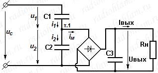
Let's assume that our load is a bridge, a smoothing capacitor and, in fact, a payload (see the figure).
At the initial turn-on, when capacitor C 3 is discharged, the value of U 2 will be equal to zero and a starting charging current will flow through the bridge, the maximum initial value of which can be found by substituting the value of U 2m equal to zero into formula (3) Istart=wC 1 Uc m). This value corresponds to the worst case, when at the moment of switching on the instantaneous value of the voltage in the network was equal to the maximum value.
With each half cycle, capacitor C 3 will charge and our voltage U 2m, equal in magnitude to the voltage on the capacitor C 3 and the voltage on the payload (we denote it as U out), will also increase until it reaches some constant value. In this case, the current through the payload will be equal to the average rectified current, i.e. I out= I nm*2/"Pi" (for sinusoidal input current).
Considering also that Uc m = U c*1.414 ( U c— effective value supply voltage), and w=2*"Pi"* f, Where f- frequency of the supply voltage in hertz, we get:
Iout = 4fC 1 ( 1,414Uc-Uout( 1+C 2 /C 1 )) , if we also take into account the drop on the bridge diodes, then the final result will be:
Iout = 4fC 1 ( 1,414Uc-(Uout+ 2Ud)( 1+C 2 /C 1 )) (4) , Where Ud- drop on one diode
From this expression we can also obtain the inverse relationship Uout(Iout):
Uout=( 1,414Uc-Iout/ 4fC 1 )/( 1+C 2 /C 1 )- 2Ud (5)
What can be seen from the last two formulas? It can be seen from them that with an increase in the current consumed by the load, the voltage across the load decreases, and with a decrease in the current consumed, it increases. By opening the load circuit (that is, taking the load current equal to zero), we find the open circuit voltage: Uout xx = 1,414Uc/( 1+C 2 /C 1 )- 2Ud(6). Obviously, the bridge and capacitor C 2 must be designed for a voltage of at least U 2m max = Uout xx + 2U d = 1,414Uc/( 1+C 2 /C 1 ) .
Strictly speaking, our calculations are not entirely flawless, because the real processes here will generally be nonlinear, but our small simplifications greatly facilitate the calculations and do not greatly affect the final result.
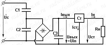
Now comes the most interesting part. I often read on the Internet that linear stabilizers do not work in such circuits, they burn out, etc., etc. Well, let's redraw our circuit once again, adding a linear voltage regulator to it (see figure).
(Ust. , In- load voltage and current).
Here our Uout (voltage on capacitor C 3) is the input voltage of the stabilizer (Uin). As we remember, in the absence of load, the output voltage will be maximum and equal to Uout xx. So it is quite obvious that for normal operation our linear stabilizer must withstand an input voltage of at least Uout xx. Or we can say it differently - the capacitors must be selected in such a way that the open-circuit output voltage (meaning the output voltage of the capacitor divider) does not burn the stabilizer when the load is accidentally disconnected (you never know, some kind of miscontact).
The maximum load current can be determined by substituting the minimum input voltage of the stabilizer into formula (4) instead of Uout. As you can see, the main thing is to calculate everything correctly, then nothing threatens the stabilizer.
This scheme is already quite working, but it has one significant drawback. In the case when we need to obtain the input voltage of the stabilizer significantly lower than the supply voltage of the network (when powered from 220 V, this is exactly what we need), the capacitance of capacitor C 2 turns out to be quite significant. A non-polar capacitor of significant capacity is quite expensive (and the dimensions are not encouraging). Is it possible to somehow use, for example, conventional electrolytic ones instead of a non-polar capacitor?
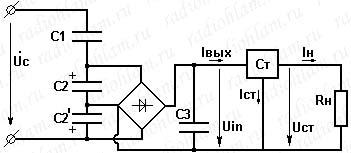
It turns out it is possible. To do this, we will redo our circuit again, in the same way as in the figure. In this circuit, instead of one capacitor C 2, two capacitors C 2 and C 2 are used (of the same capacity as in the case when there is only one capacitor C 2), isolated through bridge diodes. In this case, the reverse voltage on each of these capacitors does not exceed the voltage drop across the diode.
Despite the fact that in this case, instead of one non-polar capacitor, two electrolytic capacitors are used, such a circuit is more economical both in terms of money and size.
True, there is one nuance here. Burnout of one of the bridge diodes can result in full reverse voltage appearing on the electrolytic capacitors. If this happens, the capacitor will most likely explode.
I would also like to note that transformerless power supplies should be handled with extreme caution, since such a circuit is not isolated from the mains supply and touching its conductive parts can cause serious electric shock.
Online calculator for calculating a power supply with a capacitor divider:
(for correct calculations, use a dot rather than a comma as the decimal point)
1) Initial data:
(if you do not know the minimum input voltage of the stabilizer and the magnitude of the voltage drop across the bridge diodes, then the calculation will be made for: Uin = Ust and Ud = 0, - as if the minimum input voltage is equal to the output voltage of the stabilizer and the diodes are ideal).
Nowadays there is a lot of small-sized equipment in the house that requires constant power. These include watches with LED displays, thermometers, small-sized receivers, etc. In principle, they are designed for batteries, but they run out at the most inopportune moment. A simple way out is to power them from network power supplies. But even a small-sized network (step-down) transformer is quite heavy and takes up quite a bit of space, and switching power supplies are still complex, requiring certain experience and expensive equipment to manufacture.
A solution to this problem, if certain conditions are met, can be a transformerless power supply with a quenching capacitor. These conditions:
- complete autonomy of the powered device, i.e. no external devices should be connected to it (for example, a tape recorder to the receiver for recording a program);
- dielectric (non-conducting) housing and the same control knobs for the power supply itself and the device connected to it.
This is due to the fact that when powered from a transformerless unit, the device is under network potential, and touching its non-insulated elements can “shake” well. It is worth adding that when setting up such power supplies, you should follow safety rules and caution.
If necessary, use an oscilloscope for setup, the power supply must be connected via an isolation transformer.
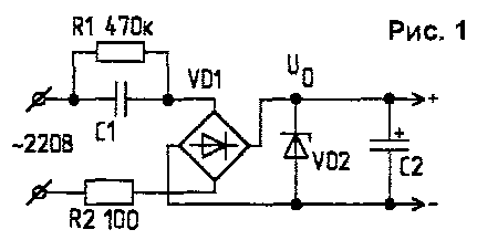
In its simplest form, the circuit of a transformerless power supply has the form shown in Fig. 1.
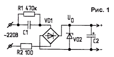
To limit the inrush current when connecting the unit to the network, resistor R2 is connected in series with capacitor C1 and rectifier bridge VD1, and resistor R1 is connected in parallel to it to discharge the capacitor after disconnection.
In general, a transformerless power supply is a symbiosis of a rectifier and a parametric stabilizer. Capacitor C1 for alternating current is a capacitive (reactive, i.e., not consuming energy) resistance Xc, the value of which is determined by the formula:
![]()
where ( - network frequency (50 Hz); C - capacitance of capacitor C1, F.
Then the output current of the source can be approximately determined as follows:
where Uc is the network voltage (220 V).
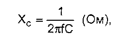
The input part of another power supply (Fig. 2a) contains a ballast capacitor C1 and a bridge rectifier made of diodes VD1, VD2 and zener diodes VD3, VD4. Resistors R1, R2 play the same role as in the first circuit. The oscillogram of the block's output voltage is shown in Fig. 2b (when the output voltage exceeds the stabilization voltage of the zener diodes, otherwise it works like a regular diode).
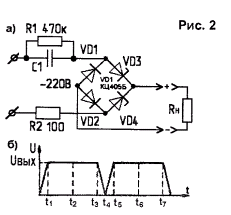
From the beginning of the positive half-cycle of the current through capacitor C1 to moment t1, the zener diode VD3 and diode VD2 are open, and the zener diode VD4 and diode VD1 are closed. In the time interval t1...t3, the zener diode VD3 and the diode VD2 remain open, and a stabilization current pulse passes through the opened zener diode VD4. The voltage at the output Uout and at the zener diode VD4 is equal to its stabilization voltage Ust.
The pulse stabilization current, which is through for a diode-zener diode rectifier, bypasses the RH load, which is connected to the bridge output. At time t2 the stabilization current reaches its maximum, and at time t3 it is zero. Until the end of the positive half-cycle, the zener diode VD3 and diode VD2 remain open.
At moment t4 the positive half-cycle ends and the negative half-cycle begins, from the beginning of which to moment t5 the zener diode VD4 and diode VD1 are already open, and the zener diode VD3 and diode VD2 are closed. In the time interval t5-t7, the zener diode VD4 and the diode VD1 continue to remain open, and a through stabilization current pulse passes through the zener diode VD3 at voltage UCT, the maximum at time t6. Starting from t7 and until the end of the negative half-cycle, the zener diode VD4 and diode VD1 remain open. The considered cycle of operation of the diode-zener diode rectifier is repeated in the following periods of mains voltage.
Thus, a rectified current passes through the zener diodes VD3, VD4 from the anode to the cathode, and a pulsed stabilization current passes in the opposite direction. In the time intervals t1...t3 and t5...t7, the stabilization voltage changes by no more than a few percent. The value of the alternating current at the input of the bridge VD1...VD4 is, to a first approximation, equal to the ratio of the network voltage to the capacitance of the ballast capacitor C1.
The operation of a diode-zener diode rectifier without a ballast capacitor, which limits the through current, is impossible. Functionally, they are inseparable and form a single whole - a capacitor-zener diode rectifier.
The spread in the UCT values of zener diodes of the same type is approximately 10%, which leads to additional ripples in the output voltage with the frequency of the supply network; the amplitude of the ripple voltage is proportional to the difference in the Ust values of zener diodes VD3 and VD4.
When using powerful zener diodes D815A...D817G, they can be installed on a common radiator if their type designation contains the letters "PP (zener diodes D815APP...D817GPP have reverse polarity of the terminals). Otherwise, the diodes and zener diodes must be swapped.
Transformerless power supplies are usually assembled according to the classical scheme: quenching capacitor, AC voltage rectifier, filter capacitor, stabilizer. A capacitive filter smoothes out output voltage ripples. The greater the capacitance of the filter capacitors, the less ripple and, accordingly, the greater the constant component of the output voltage. However, in some cases you can do without a filter, which is often the most cumbersome component of such a power source.
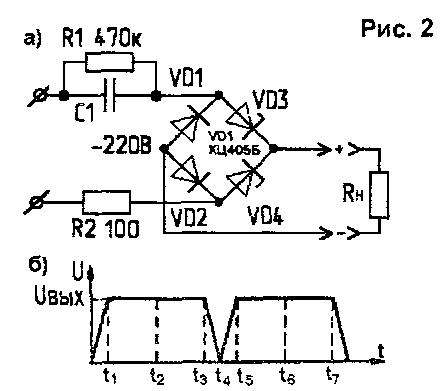
It is known that a capacitor connected to an alternating current circuit shifts its phase by 90°. A phase-shifting capacitor is used, for example, when connecting a three-phase motor to a single-phase network. If you use a phase-shifting capacitor in the rectifier, which ensures mutual overlap of half-waves of the rectified voltage, in many cases you can do without a bulky capacitive filter or significantly reduce its capacitance. The circuit of such a stabilized rectifier is shown in Fig. 3.
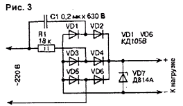
The three-phase rectifier VD1.VD6 is connected to an alternating voltage source through active (resistor R1) and capacitive (capacitor C1) resistances.
The output voltage of the rectifier stabilizes the zener diode VD7. Phase-shifting capacitor C1 must be designed for operation in alternating current circuits. Here, for example, capacitors of the K73-17 type with an operating voltage of at least 400 V are suitable.
This rectifier can be used where it is necessary to reduce the dimensions electronic device, since the dimensions of the oxide capacitors of a capacitive filter are, as a rule, much larger than those of a phase-shifting capacitor of a relatively small capacity.
Another advantage of the proposed option is that the current consumption is almost constant (in the case of a constant load), whereas in rectifiers with a capacitive filter, at the moment of switching on, the starting current significantly exceeds the steady-state value (due to the charge of the filter capacitors), which in some cases is extremely undesirable .
The described device can also be used with series voltage stabilizers that have a constant load, as well as with a load that does not require voltage stabilization.
A completely simple transformerless power supply (Fig. 4) can be built “on the knee” in literally half an hour.
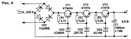
In this embodiment, the circuit is designed for an output voltage of 6.8 V and a current of 300 mA. The voltage can be changed by replacing the zener diode VD4 and, if necessary, VD3. And by installing transistors on radiators, you can increase the load current. Diode bridge - any one designed for a reverse voltage of at least 400 V. By the way, you can also remember about the “ancient” diodes. D226B.
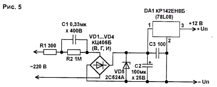
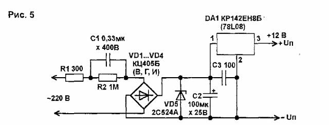
In another transformerless source (Fig. 5), the KR142EN8 microcircuit is used as a stabilizer. Its output voltage is 12 V. If adjustment of the output voltage is necessary, then pin 2 of the DA1 microcircuit is connected to the common wire through a variable resistor, for example, type SPO-1 (with a linear characteristic of resistance change). Then the output voltage can vary in the range of 12...22 V.
As a DA1 microcircuit, to obtain other output voltages, you need to use the appropriate integrated stabilizers, for example, KR142EN5, KR1212EN5, KR1157EN5A, etc. Capacitor C1 must have an operating voltage of at least 300 V, brand K76-3, K73-17 or similar (non-polar , high voltage). Oxide capacitor C2 acts as a power supply filter and smoothes out voltage ripples. Capacitor C3 reduces high frequency interference. Resistors R1, R2 are MLT-0.25 type. Diodes VD1...VD4 can be replaced with KD105B...KD105G, KD103A, B, KD202E. Zener diode VD5 with a stabilization voltage of 22...27 V protects the microcircuit from voltage surges when the source is turned on.
Despite the fact that theoretically capacitors in an AC circuit do not consume power, in reality they can generate some heat due to losses. You can check the suitability of a capacitor as a damping capacitor for use in a transformerless source by simply connecting it to the mains and assessing the temperature of the case after half an hour. If the capacitor manages to warm up noticeably, it is not suitable. Special capacitors for industrial electrical installations practically do not heat up (they are designed for high reactive power). Such capacitors are usually used in fluorescent lamps, in ballasts of asynchronous electric motors, etc.
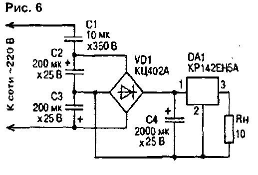
In a 5-volt source (Fig. 6) with a load current of up to 0.3 A, a capacitor voltage divider is used. It consists of a paper capacitor C1 and two oxide capacitors C2 and C3, forming the lower (according to the circuit) non-polar arm with a capacity of 100 μF (counter-series connection of capacitors). The polarizing diodes for the oxide pair are bridge diodes. With the indicated ratings of the elements, the short circuit current at the output of the power supply is 600 mA, the voltage on capacitor C4 in the absence of load is 27 V.

The power supply unit for the portable receiver (Fig. 7) easily fits into its battery compartment. The diode bridge VD1 is designed for operating current, its maximum voltage is determined by the voltage provided by the zener diode VD2. Elements R3, VD2. VT1 form an analogue of a powerful zener diode. The maximum current and power dissipation of such a zener diode are determined by transistor VT1. It may require a heatsink. But in any case, the maximum current of this transistor should not be less than the load current. Elements R4, VD3 - circuit indicating the presence of output voltage. At low load currents, it is necessary to take into account the current consumed by this circuit. Resistor R5 loads the power circuit with a low current, which stabilizes its operation.

Quenching capacitors C1 and C2 are KBG type or similar. You can also use K73-17 with an operating voltage of 400 V (250 V is also suitable, since they are connected in series). The output voltage depends on the resistance of the quenching capacitors alternating current, real load current and stabilization voltage of the zener diode.
To stabilize the voltage of a transformerless power supply with a quenching capacitor, you can use symmetrical dinistors (Fig. 8).
![]()
When the filter capacitor C2 is charged to the opening voltage of the dinistor VS1, it turns on and bypasses the input of the diode bridge. The load at this time receives power from capacitor C2. At the beginning of the next half-cycle, C2 is again recharged to the same voltage, and the process is repeated. The initial discharge voltage of capacitor C2 does not depend on the load current and network voltage, therefore the stability of the unit’s output voltage is quite high.
The voltage drop across the dinistor when turned on is small, the power dissipation, and therefore its heating, is significantly less than that of a zener diode. The maximum current through the dinistor is about 60 mA. If this value is not enough to obtain the required output current, you can “power up the dinistor with a triac or thyristor (Fig. 9). The disadvantage of such power supplies is the limited choice of output voltages, determined by the switching voltages of the dinistors.
A transformerless power supply with adjustable output voltage is shown in Fig. 10a.
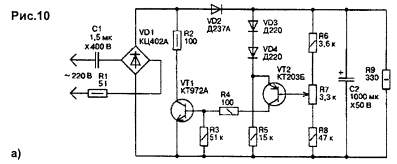
Its feature is the use of adjustable negative feedback from the block output to transistor stage VT1 connected in parallel to the output of the diode bridge. This stage is a regulatory element and is controlled by a signal from the output of a single-stage amplifier to VT2.
The output signal VT2 depends on the voltage difference supplied from the variable resistor R7, connected in parallel with the output of the power supply, and the reference voltage source on the diodes VD3, VD4. Essentially, the circuit is an adjustable parallel regulator. The role of the ballast resistor is played by the quenching capacitor C1, the parallel controlled element is played by the transistor VT1.
This power supply works as follows.
When connected to the network, transistors VT1 and VT2 are locked, and the storage capacitor C2 is charged through the diode VD2. When the base of transistor VT2 reaches a voltage equal to the reference voltage on diodes VD3, VD4, transistors VT2 and VT1 are unlocked. Transistor VT1 shunts the output of the diode bridge, and its output voltage drops, which leads to a decrease in the voltage on the storage capacitor C2 and to the blocking of transistors VT2 and VT1. This, in turn, causes an increase in voltage on C2, unlocking VT2, VT1 and repeating the cycle.
Due to the negative feedback operating in this way, the output voltage remains constant (stabilized) both with the load on (R9) and without it (at idle). Its value depends on the position of the potentiometer R7.
The upper (according to the diagram) position of the engine corresponds to a higher output voltage. The maximum output power of the given device is 2 W. The output voltage adjustment limits are from 16 to 26 V, and with a short-circuited diode VD4 - from 15 to 19.5 V. The level of ripple on the load is no more than 70 mV.
Transistor VT1 operates in alternating mode: when there is a load - in linear mode, at idle - in pulse-width modulation (PWM) mode with a voltage pulsation frequency on capacitor C2 of 100 Hz. In this case, the voltage pulses on the VT1 collector have flat edges.
The criterion for the correct choice of capacitance C1 is to obtain the required maximum voltage at the load. If its capacity is reduced, then the maximum output voltage at the rated load is not achieved. Another criterion for choosing C1 is the constancy of the voltage oscillogram at the output of the diode bridge (Fig. 10b).
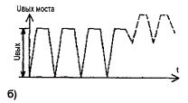
The voltage oscillogram has the form of a sequence of rectified sinusoidal half-waves of the mains voltage with limited (flattened) peaks of positive half-sine waves; the amplitude of the peaks is a variable value, depending on the position of the R7 slider, and changes linearly as it rotates. But each half-wave must necessarily reach zero; the presence of a constant component (as shown in Fig. 10b by the dotted line) is not allowed, because in this case, the stabilization regime is violated.
The linear mode is lightweight, transistor VT1 heats up little and can operate practically without a heatsink. Slight heating occurs in the lower position of the R7 engine (at minimum output voltage). At idle, the thermal regime of transistor VT1 worsens in the upper position of the R7 engine. In this case, transistor VT1 should be installed on a small radiator, for example, in the form of a “flag” made of a square aluminum plate with a side of 30 mm and a thickness of 1...2 mm.
Regulating transistor VT1 is of medium power, with a high transmission coefficient. Its collector current must be 2...3 times greater than the maximum load current, the permissible collector-emitter voltage must be no less than the maximum output voltage of the power supply. Transistors KT972A, KT829A, KT827A, etc. can be used as VT1. Transistor VT2 operates in low current mode, so any low-power pnp transistor is suitable - KT203, KT361, etc.
Resistors R1, R2 are protective. They protect the control transistor VT1 from failure due to current overload during transient processes when the unit is connected to the network.
The transformerless capacitor rectifier (Fig. 11) operates with auto-stabilization of the output voltage. This is achieved by changing the connection time of the diode bridge to the storage capacitor. Transistor VT1, operating in switch mode, is connected parallel to the output of the diode bridge. Base VT1 is connected via zener diode VD3 to storage capacitor C2, separated by DC from the bridge output with diode VD2 to prevent rapid discharge when VT1 is open. As long as the voltage at C2 is less than the stabilization voltage VD3, the rectifier operates as usual. When the voltage on C2 increases and VD3 opens, transistor VT1 also opens and shunts the output of the rectifier bridge. The voltage at the bridge output decreases abruptly to almost zero, which leads to a decrease in the voltage at C2 and the zener diode and the key transistor are turned off.
![]()
Next, the voltage on capacitor C2 increases again until the zener diode and transistor are turned on, etc. The process of auto-stabilization of the output voltage is very similar to the operation of a pulse voltage stabilizer with pulse-width regulation. Only in the proposed device the pulse repetition rate is equal to the voltage ripple frequency at C2. To reduce losses, the key transistor VT1 must have a high gain, for example, KT972A, KT829A, KT827A, etc. You can increase the output voltage of the rectifier by using a higher-voltage zener diode (a chain of low-voltage ones connected in series). With two zener diodes D814V, D814D and a capacitance of capacitor C1 of 2 μF, the output voltage across a load with a resistance of 250 Ohms can be 23...24 V.
Similarly, you can stabilize the output voltage of a half-wave diode-capacitor rectifier (Fig. 12).
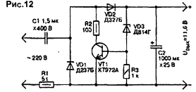
For a rectifier with a positive output voltage, an n-p-n transistor is connected in parallel with the diode VD1, controlled from the output of the rectifier through a zener diode VD3. When capacitor C2 reaches a voltage corresponding to the moment the zener diode opens, transistor VT1 also opens. As a result, the amplitude of the positive half-wave voltage supplied to C2 through the diode VD2 is reduced to almost zero. When the voltage on C2 decreases, transistor VT1 closes thanks to the zener diode, which leads to an increase in the output voltage. The process is accompanied by pulse-width regulation of the pulse duration at input VD2, therefore, the voltage on capacitor C2 is stabilized.
In a rectifier with a negative output voltage, a pnp transistor KT973A or KT825A must be connected in parallel with the diode VD1. The output stabilized voltage on a load with a resistance of 470 Ohms is about 11 V, the ripple voltage is 0.3...0.4 V.
In both options, the zener diode operates in a pulsed mode at a current of a few milliamps, which is in no way related to the rectifier load current, the variation in the capacitance of the quenching capacitor and fluctuations in the network voltage. Therefore, losses in it are significantly reduced, and it does not require a heat sink. The key transistor also does not require a radiator.
Resistors R1, R2 in these circuits limit the input current during transient processes at the moment the device is connected to the network. Due to the inevitable “bouncing” of the contacts of the power plug, the switching process is accompanied by a series of short-term short circuits and open circuits. During one of these short circuits, the quenching capacitor C1 can be charged to the full amplitude value of the network voltage, i.e. up to approximately 300 V. After a break and subsequent closure of the circuit due to “bouncing”, this and the mains voltage can add up and amount to a total of about 600 V. This is the worst case, which must be taken into account to ensure reliable operation of the device.
Another version of the key transformerless power supply circuit is shown in Fig. 13.
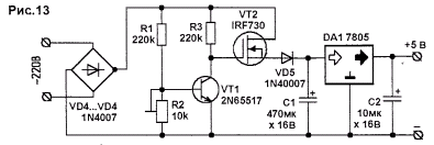
The mains voltage, passing through the diode bridge on VD1.VD4, is converted into a pulsating amplitude of about 300 V. Transistor VT1 is a comparator, VT2 is a switch. Resistors R1, R2 form a voltage divider for VT1. By adjusting R2 you can set the response voltage of the comparator. Until the voltage at the output of the diode bridge reaches the set threshold, the transistor VT1 is closed, the gate VT2 has an unlocking voltage and is open. Capacitor C1 is charged through VT2 and diode VD5.
When the set operating threshold is reached, transistor VT1 opens and bypasses the gate VT2. The key closes and will open again when the voltage at the bridge output becomes less than the comparator operating threshold. Thus, a voltage is set at C1, which is stabilized by the integrated stabilizer DA1.
With the ratings shown in the diagram, the source provides an output voltage of 5 V at a current of up to 100 mA. The setting consists of setting the response threshold VT1. You can use IRF730 instead. KP752A, IRF720, BUZ60, 2N6517 is replaced by KT504A.
A miniature transformerless power supply for low-power devices can be built on the HV-2405E chip (Fig. 14), which directly converts alternating voltage to direct voltage.
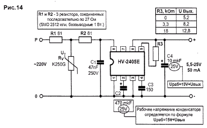
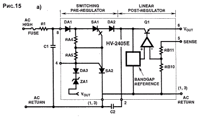
The input voltage range of the IC is -15...275 V. The output voltage range is 5...24 V with a maximum output current of up to 50 mA. Available in a flat plastic housing DIP-8. The structure of the microcircuit is shown in Fig. 15a, the pinout is shown in Fig. 15b.

In the source circuit (Fig. 14), special attention should be paid to resistors R1 and R2. Their total resistance should be around 150 Ohms, and the dissipated power should be at least 3 W. The input high-voltage capacitor C1 can have a capacitance from 0.033 to 0.1 μF. Varistor Rv can be used in almost any type with an operating voltage of 230.250 V. Resistor R3 is selected depending on the required output voltage. In its absence (outputs 5 and 6 are closed), the output voltage is slightly more than 5 V; with a resistance of 20 kOhm, the output voltage is about 23 V. Instead of a resistor, you can turn on a zener diode with the required stabilization voltage (from 5 to 21 V). There are no special requirements for other parts, with the exception of the choice of operating voltage of electrolytic capacitors (calculation formulas are shown in the diagram).
Considering the potential danger of transformerless sources, in some cases a compromise option may be of interest: with a quenching capacitor and a transformer (Fig. 16).
![]()
A transformer with high voltage is suitable here. secondary winding, since the required rectified voltage is set by selecting the capacitance of capacitor C1. The main thing is that the transformer windings provide the required current.
To prevent the device from malfunctioning when the load is disconnected, a D815P zener diode should be connected to the output of the VD1...VD4 bridge. In normal mode, it does not work, since its stabilization voltage is higher than the operating voltage at the bridge output. Fuse FU1 protects the transformer and stabilizer in case of breakdown of capacitor C1.
In sources of this type, voltage resonance may occur in a circuit of series-connected capacitive (capacitor C1) and inductive (transformer T1) resistances. This should be remembered when setting them up and monitoring the voltages with an oscilloscope.
See other articles section.
Read and write useful
MAINS POWER SUPPLY WITH DURING CAPACITOR
Many of the devices described above used transformerless power supplies with a quenching capacitor. They are convenient due to their simplicity, small size and weight, but are not always applicable due to the galvanic connection of the output circuit to the 220 V network. How to correctly calculate such a source is described in this section.
In a transformerless power supply, a series-connected capacitor and load are connected to an alternating voltage network. Let us first consider the operation of a source with a purely resistive load (Fig. 123a).
In amateur radio practice, a source is often used in which a quenching capacitor is connected to the network in series with
diode bridge, and the load, shunted by another capacitor, is powered from the output diagonal of the bridge (Fig. 124). In this case, the circuit becomes sharply nonlinear and the shape of the current flowing through the bridge and the quenching capacitor will differ from
sinusoidal. Because of this, the calculation presented above is incorrect.
What are the processes occurring in a source with a smoothing capacitor C2 with a capacitance sufficient to consider the output voltage ripple to be negligible? For the damping capacitor C1, the diode bridge (together with C2 and Rн) in steady state is a kind of equivalent of a symmetrical zener diode. When the voltage at this equivalent is less than a certain value (it is almost equal to the voltage Uout on capacitor C2), the bridge is closed and no current passes through it; if it is higher, current flows through the open bridge, preventing the voltage at the bridge input from increasing.
We will begin our consideration from moment t1, when the network voltage is maximum (Fig. 125). Capacitor C1 is charged to the amplitude voltage of the network Us.amp minus the voltage on the diode bridge Um, approximately equal to Uout. The current through capacitor C1 and the closed bridge is zero. The voltage in the network decreases according to a cosine law (graph 1), on the bridge it also decreases (graph 2), and the voltage on capacitor C1 does not change.
The capacitor current will remain zero until the voltage on the diode bridge, changing sign to the opposite, reaches the value -Uout (moment t2). At this moment, current Ic1 appears abruptly through capacitor C1 and the bridge. Starting from moment t2, the voltage on the bridge does not change, and the current is determined by the rate of change of the network voltage and, therefore, will be exactly the same as if only capacitor C1 was connected to the network (graph 3).
When the network voltage reaches a negative amplitude value (moment tз), the current through capacitor C1 will again become zero. The process is then repeated every half-cycle.
The current through the bridge flows only in the time interval t2-t3, its average value can be calculated as the area of the shaded part
In the absence of a zener diode for the required voltage Uout;
allowing the calculated maximum stabilization current, you can connect several zener diodes at a lower voltage in series.
The minimum load current In nun should be substituted into formula (4) only when this current is long-lasting - a few seconds or more. With a short-term minimum load current (fractions of a second), it must be replaced with an average (over time) load current. If the zener diode allows a current greater than that calculated by formula (4), it is advisable to use a damping capacitor slightly
source according to the diagram in Fig. 124 charging this capacitor lasts a quarter of the period of the mains voltage, and the same amount of time - discharging. With this approximation, the double ripple voltage 2Uп (peak-to-peak) is equal to: 2п=0.25In max/fС.
2Up=0.75Inmax/fC.
For an output voltage less than 100 V, charging actually takes longer, discharging takes less time, and these expressions give a noticeably overestimated result, so calculating the capacity of the smoothing capacitor using the formulas obtained from them provides some margin: C = 5Inmax/2Up (for Fig. 124); C = 15Inmax/2Up (for Fig. 126), where current is in milliamps, capacitance is in microfarads, voltage is in volts.
Although the zener diode reduces the ripple voltage, it is not recommended to use a smoothing capacitor with a capacitance less than that calculated. In the previously considered example, with a ripple swing of 0.2 V, the capacitance of the smoothing capacitor is equal to:
C2=5*15/0.2=375 µF.
To limit the current surge through the diodes of the rectifier bridge at the moment the source is connected to the network in series with the quenching capacitor, it is necessary to include a current-limiting resistor. The lower the resistance of this resistor, the lower the losses in it. For a KTs407A diode bridge or a bridge of KD103A diodes, a resistor with a resistance of 36 Ohms is sufficient.
The average power P dissipated on it can be determined by the formula: P = 5.6C1^2R, where capacity is in microfarads, resistance is in ohms, power is in milliwatts. For the example discussed above, P=5.6*0.39^236=30 mW. For reliability (after all, at the moment of switching on, an amplitude mains voltage can be applied to the resistor), it is recommended to use a resistor with a power of at least 0.5 W.
In order to exclude the possibility of electric shock when setting up devices with the sources in question, they should be powered not from the mains, but from a network laboratory low-voltage power supply through a current-limiting resistor. Output voltage laboratory block set more supply voltage to the device being adjusted so that the current through the current-limiting resistor is close to Ist min+ Inmax.
Sometimes it is convenient to use a source resistor as a current-limiting resistor, limiting the current surge through the diodes of the rectifier bridge. In this case, it is enough to short-circuit the conclusions
(Fig. 130) for load current up to 0.3 A and an uninterruptible power supply for electronic-mechanical watches (Fig. 131).
The voltage divider of a five-volt source consists of a paper capacitor C1 and two oxide capacitors C2 and S3, forming the lower non-polar arm with a capacity of 100 microfarads. The polarizing diodes for the oxide pair are the left-hand bridge diodes in the circuit. With the ratings of the elements indicated in the diagram, the circuit current (at Rн=O) is 600 mA, the voltage on capacitor C4 in the absence of load is 27 V.
Electromechanical watches are usually powered by a single galva
nic element with a voltage of 1.5 V. The proposed source produces a voltage of 1.4 V with an average load current of 1 mA. The voltage removed from the divider C1C2 straightens the node on the elements VD1, VD2, SZ. Without load, the voltage on the capacitor SZ does not exceed 12 V.
The transistor VT1, connected by the emitter follower, and the galvanic element G1 make up the voltage stabilizer. The output of the source will be the element voltage minus the voltage drop across the emitter junction of the transistor.
The current consumed from element G1 in the presence of mains voltage is h21 times less than the load current, which significantly extends the service life of the element. In practice, this means that the element has to be replaced not because it is discharged by the load current, but due to other reasons - self-discharge, drying out of the electrolyte, etc.
In the event of a power failure in the network, the transistor exits the emitter follower mode and the load is supplied by the galvanic element G1 through the open emitter junction. After the mains voltage appears, the transistor returns to emitter follower mode and the load switches to mains power. Capacitor C4 ensures normal operation of the clock when element G1 is deeply discharged.
The D223 diodes can be replaced with any others, the MP41A transistor can be replaced with any germanium p-n-p structures. Element G1
It is better to use alkaline, for example, Duracell, Energizer. The actual service life of such an element in a power supply can reach 10 years.
And one last thing. The design of transformerless sources and devices powered from them must exclude the possibility of touching any conductors during operation. Particular attention should be paid to insulating the controls.
Nowadays there is a lot of small-sized equipment in the house that requires constant power. These include watches with LED displays, thermometers, small-sized receivers, etc. In principle, they are designed for batteries, but they run out at the most inopportune moment. A simple way out is to power them from network power supplies. But even a small-sized network (step-down) transformer is quite heavy and takes up quite a bit of space. A pulsed sources Supplies are still complex and require some experience and expensive equipment to manufacture.
A solution to this problem, if certain conditions are met, can be a transformerless power supply with a quenching capacitor. These conditions are...
Full autonomy of the powered device, i.e. no external devices should be connected to it (for example, a tape recorder for recording a program to the receiver); - a dielectric (non-conducting) case and the same control knobs on the power supply itself and the device connected to it.
This is due to the fact that when powered from a transformerless unit, the device is under network potential, and touching its non-insulated elements can “shake” well. It is worth adding that when setting up such power supplies, you should follow safety rules and caution. If necessary, use an oscilloscope for setup, the power supply must be connected via an isolation transformer.
In its simplest form, the circuit of a transformerless power supply has the form shown in Fig. 1.
To limit the inrush current when connecting the unit to the network, resistor R2 is connected in series with capacitor C1 and rectifier bridge VD1, and resistor R1 is connected in parallel to it to discharge the capacitor after disconnection.
In general, a transformerless power supply is a symbiosis of a rectifier and a parametric stabilizer. Capacitor C1 for alternating current is a capacitive (reactive, i.e., not consuming energy) resistance Xc, the value of which is determined by the formula:
where f is the network frequency (50 Hz); C is the capacitance of the capacitor C1, F. Then the output current of the source can be approximately determined as follows:

where Uc is the network voltage (220 V).
The input part of another power supply (Fig. 2a) contains a ballast capacitor C1 and a bridge rectifier consisting of diodes VD1, VD2 and zener diodes VD3, VD4. Resistors R1, R2 play the same role as in the first circuit. The oscillogram of the block's output voltage is shown in Fig. 2b (when the output voltage exceeds the stabilization voltage of the zener diodes, otherwise it works like a regular diode).
From the beginning of the positive half-cycle of the current through capacitor C1 to the moment ti, the zener diode VD3 and diode \U2 are open, and the zener diode VD4 and diode V01 are closed. In the time interval ti...t3, the zener diode VD3 and the diode VD2 remain open, and a stabilization current pulse passes through the opened zener diode VD4. The voltage at the output and at the zener diode VD4 is equal to its stabilization voltage UCT.
The pulse stabilization current, which is through for the diode-zener rectifier, bypasses the RH load, which is connected to the bridge output. At moment t2 the stabilization current reaches its maximum, and at moment 13 it is equal to zero. Until the end of the positive half-cycle, the zener diode VD3 and diode VD2 remain open.
At moment t4 the positive half-cycle ends and the negative half-cycle begins, from the beginning of which to moment ts the zener diode VD4 and diode VD1 are already open, and the zener diode VD3 and diode VD2 are closed. In the time interval ts-.ty, the zener diode VD4 and diode VD1 continue to remain open, and through the zener diode VD3 at voltage UCT a through pulse of stabilization current passes, maximum at the moment te- Starting from 1uid until the end of the negative half-cycle, the zener diode VD4 and diode VD1 remain open. The considered cycle of operation of the diode-stabilizer rectifier is repeated in the following periods of mains voltage.
Thus, a rectified current passes through the zener diodes VD3, VD4 from the anode to the cathode, and a pulsed stabilization current passes in the opposite direction. In the time intervals t-j...ts and tg.^ty, the stabilization voltage changes by no more than a few percent. The value of the alternating current at the input of the bridge VD1...VD4 is, to a first approximation, equal to the ratio of the network voltage to the capacitance of the ballast capacitor C1.
The operation of a diode-zener rectifier without a ballast capacitor, which limits the through current, is impossible. Functionally, they are inseparable and form a single whole - a capacitor-zener diode rectifier.
The spread in the UCT values of zener diodes of the same type is approximately 10%, which leads to additional ripples in the output voltage with the frequency of the supply network. The amplitude of the ripple voltage is proportional to the difference in the UCT values of the zener diodes VD3 and VD4.
When using powerful zener diodes D815A...D817G, they can be installed on a common radiator if their type designation contains the letters "PP" (zener diodes D815APP...D817GPP have reverse polarity of the terminals). Otherwise, the diodes and zener diodes must be swapped.
Transformerless power supplies are usually assembled according to the classical scheme: quenching capacitor, AC voltage rectifier, filter capacitor, stabilizer. A capacitive filter smoothes out output voltage ripples. The greater the capacitance of the filter capacitors, the less ripple and, accordingly, the greater the constant component of the output voltage. However, in some cases you can do without a filter, which is often the most cumbersome component of such a power source.
It is known that a capacitor connected to an alternating current circuit shifts its phase by 90°. A phase-shifting capacitor is used, for example, when connecting a three-phase motor to a single-phase network. If you use a phase-shifting capacitor in the rectifier, which ensures mutual overlap of half-waves of the rectified voltage, in many cases you can do without a bulky capacitive filter or significantly reduce its capacitance. The circuit of such a stabilized rectifier is shown in Fig. 3.
The three-phase rectifier VD1 ... VD6 is connected to an alternating voltage source through active (resistor R1) and capacitive (capacitor C1) resistances.
Such a rectifier can be used where it is necessary to reduce the dimensions of an electronic device, since the dimensions of the oxide capacitors of a capacitive filter are, as a rule, much larger than those of a relatively small phase-shifting capacitor.
Another advantage of the proposed option is that the current consumption is almost constant (in the case of a constant load), whereas in rectifiers with a capacitive filter, at the moment of switching on, the starting current significantly exceeds the steady-state value (due to the charge of the filter capacitors), which in some cases is extremely undesirable .
The described device can also be used with series voltage stabilizers that have a constant load, as well as with a load that does not require voltage stabilization.
A completely simple transformerless power supply (Fig. 4) can be built “on the knee” in literally half an hour. In this embodiment, the circuit is designed for an output voltage of 6.8 V and a current of 300 mA. The voltage can be changed by replacing the zener diode VD4 and, if necessary, VD3. And by installing transistors on radiators, you can increase the load current. Diode bridge - any one designed for a reverse voltage of at least 400 V. By the way, you can also remember the “ancient” D226B diodes.

In another transformerless source (Fig. 5), the KR142EN8 microcircuit is used as a stabilizer. Its output voltage is 12 V. If adjustment of the output voltage is necessary, then pin 2 of the DA1 microcircuit is connected to the common wire through a variable resistor, for example, type SPO-1 (with a linear characteristic of resistance change). Then the output voltage can vary in the range of 12...22 V.
As a DA1 microcircuit, to obtain other output voltages, you need to use the appropriate integrated stabilizers, for example, KR142EN5, KR1212EN5, KR1157EN5A, etc. Capacitor C1 must be for an operating voltage of at least 300 V, brand K76-3, K73-17 or similar (non-polar , high voltage). Oxide capacitor C2 acts as a power supply filter and smoothes out voltage ripples. Capacitor SZ reduces high frequency interference. Resistors R1, R2 are MLT-0.25 type. Diodes VD1...VD4 can be replaced with KD105B...KD105G, KD103A, B, KD202E. Zener diode VD5 with a stabilization voltage of 22...27 V protects the microcircuit from voltage surges when the source is turned on.
Despite the fact that, theoretically, capacitors in an alternating current circuit do not consume any power, in reality, due to the presence of losses, a certain amount of heat may be released in them. You can check the suitability of a capacitor as a damping capacitor for use in a transformerless source by simply connecting it to the mains and assessing the temperature of the case after half an hour. If the capacitor manages to warm up noticeably, it is not suitable. Special capacitors for industrial electrical installations practically do not heat up (they are designed for high reactive power). Such capacitors are usually used in fluorescent lamps, in starters and control devices of asynchronous electric motors, etc.
In a 5-volt source (Fig. 6) with a load current of up to 0.3 A, a capacitor voltage divider is used. It consists of a paper capacitor C1 and two oxide capacitors C2 and SZ, forming the lower (according to the circuit) non-polar arm with a capacity of 100 μF (counter-series connection of capacitors). The polarizing diodes for the oxide pair are bridge diodes. With the indicated ratings of the elements, the short circuit current at the output of the power supply is 600 mA, the voltage on capacitor C4 in the absence of load is 27 V.
The power supply unit for the portable receiver (Fig. 7) easily fits into its battery compartment. The diode bridge VD1 is designed for operating current, its maximum voltage is determined by the voltage provided by the zener diode VD2. Elements R3, VD2, VT1 form an analogue of a powerful zener diode. The maximum current and power dissipation of such a zener diode are determined by transistor VT1. It may require a heatsink. But in any case, the maximum current of this transistor should not be less than the load current. Elements R4, VD3 - presence indication circuit
output voltage. At low load currents, it is necessary to take into account the current consumed by this circuit. Resistor R5 loads the power circuit with a low current, which stabilizes its operation.
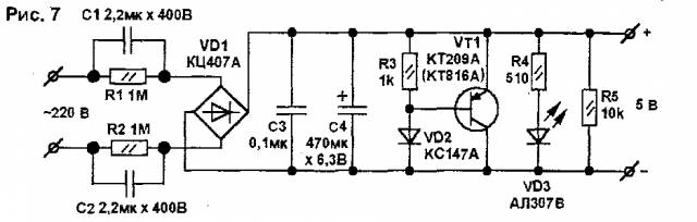
Quenching capacitors C1 and C2 are KBG type or similar. You can also use K73-17 with an operating voltage of 400 V (250 V is also suitable, since they are connected in series). The output voltage depends on the resistance of the quenching capacitors to alternating current, the actual load current and the stabilization voltage of the zener diode.
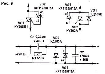
To stabilize the voltage of a transformerless power supply with a quenching capacitor, you can use symmetrical dinistors (Fig. 8).
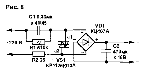
When the filter capacitor C2 is charged to the opening voltage of the dinistor VS1, it turns on and bypasses the input of the diode bridge. The load at this time receives power from capacitor C2. At the beginning of the next half-cycle, C2 is recharged to the same voltage, and the process is repeated. The initial discharge voltage of capacitor C2 does not depend on the load current and network voltage, therefore the stability of the unit’s output voltage is quite high. The voltage drop across the dinistor when turned on is small, the power dissipation, and therefore its heating, is significantly less than that of a zener diode. The maximum current through the dinistor is about 60 mA. If this value is not enough to obtain the required output current, you can “power up” the dinistor with a triac or thyristor (Fig. 9). The disadvantage of such power supplies is the limited choice of output voltages, determined by the switching voltages of the dinistors.
Transformerless power supplies are easier to manufacture and cheaper than transformer ones, but they pose a certain danger to human life during setup, repair and operation. Careless touching of the live part and the grounded surface at the same time can end very disastrously.
Circuits without galvanic isolation are used in those structures where constant human presence is not required or reliable isolation from electric shock is ensured. It is worth noting that it is advisable to use such power supplies only at low load currents, since otherwise the size and cost of the necessary components grow very quickly.
There are the following types of transformerless power supplies:
- with a ballast resistor in the input circuit;
- with a ballast capacitor in the input circuit;
- with a pulse non-isolated AC/DC converter.
Ballast resistors and capacitors suppress excess mains voltage. Accordingly, resistors must be designed for high power dissipation, and capacitors must be film, for example, K73-17, preferably with an operating voltage of at least 630 V. The margin is needed because the permissible AC voltage CAS at a frequency of 50 Hz for this class of capacitors is significantly less than permissible DC voltage KDC (Table 6.2).
Ballast-type circuits “do not like” frequent switching on/off, since voltage surges occur at the initial moment of time. If possible, it is better to do without a network switch altogether, which will significantly extend the life of the device. The optimal scope of application for ballast circuits is low-power devices with round-the-clock operation.
Pulse network transformerless voltage converters are called AC/DC (“variable” AC to “constant” DC). They provide high efficiency and small dimensions, but generate pulsed noise of a fairly high frequency and amplitude. In addition, the microcircuits used in these converters are not cheap and widespread.
In Fig. 6.3, a...m shows transformerless power supply circuits with ballast resistors and capacitors, and Fig. 6.4, a...g - with microcircuits of pulsed AC/DC converters.
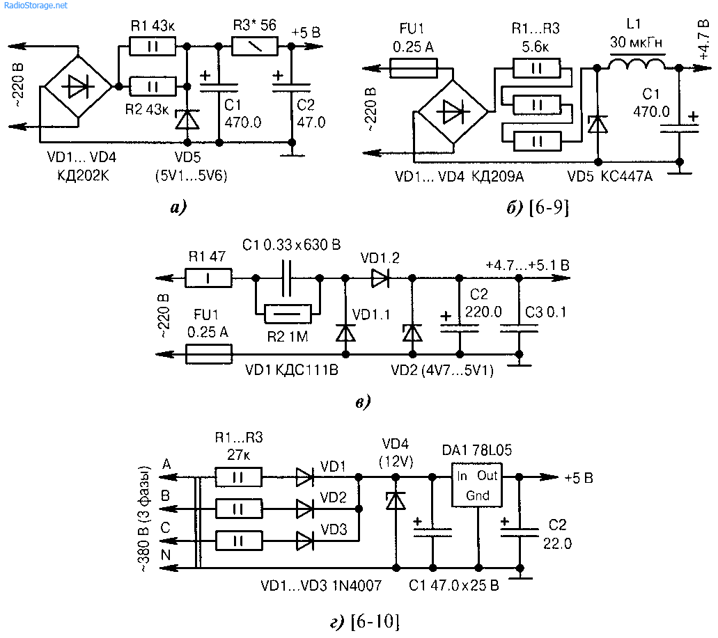
Rice. 6.3. Transformerless power supply circuits with ballast elements (beginning):
a) diodes VD1...VD4 must withstand a reverse voltage of at least 400 V. Resistors Rl, R2 are ballast for the zener diode VD5. The resistance of resistor R3 is selected so that the output voltage does not exceed +5.25 V at any load current. The low-pass filter on elements C1, R3, C2 smooths out network ripples at double frequency 100 Hz;
b) similar to Fig. 6.3, a, but the parallel ballast resistors are replaced by series-connected resistors RL..R3, the RC filter is replaced by the LC filter LI, C1, and the FUI fuse is added. The maximum permissible current through the LI inductor must be greater than the load current by a margin;
c) complete classical circuit of a power supply with ballast capacitor C1. Resistor R1 limits the initial charging current of capacitor C2 and is mandatory in such circuits. Resistor R2 quickly discharges capacitor C1 after disconnecting the plug from the 220 V network. The VD1 diode assembly rectifies the voltage and can be replaced with two diodes of type 1 N4004... 1 N4007. Capacitor C2 smoothes out network ripples, and capacitor SZ eliminates RF interference. The output voltage depends on the parameters of the zener diode VD2 and the load current;
d) food from three-phase network through ballast resistors RL..R3. Zener diode VD4 is needed so that the DA1 microcircuit does not fail from a high input voltage when the load in the +5 V circuit is interrupted or when the current consumption sharply decreases;
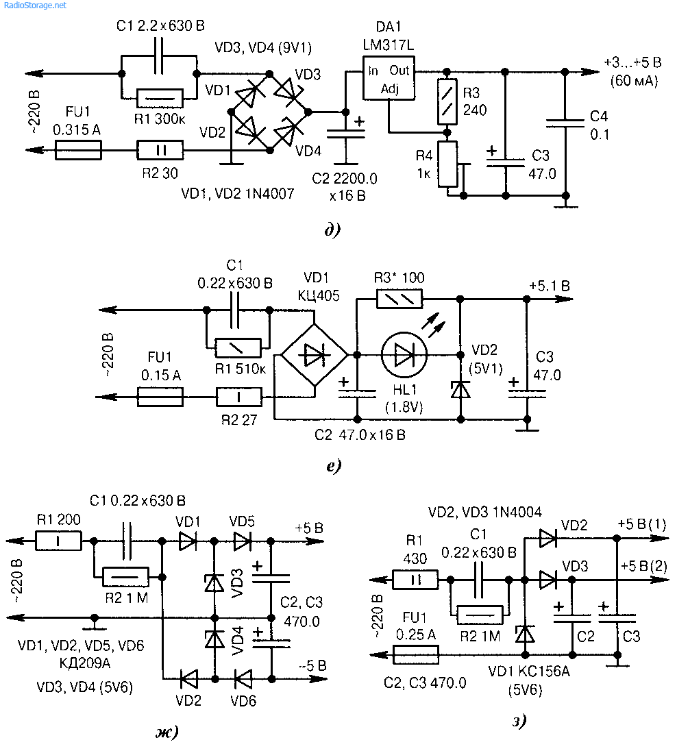
Rice. 6.3. Transformerless power supply circuits with ballast elements (continued):
e) Zener diodes VD3, VD4 have increased power dissipation of 1...3 W and perform preliminary voltage limitation. The stabilizer on the DA I chip provides the output voltage;
f) full-wave rectifier with diode bridge VD1 and LED indication of power availability. Resistor R3 determines the current in the load, as well as the brightness of the HLI indicator. The output voltage depends on the parameters of the zener diode VD2 and the load current;
g) bipolar power supply. For complete symmetry of the circuit, it is desirable to provide equal current loads along the +5 and -5 V circuits;
h) dividing the output voltage into two separate branches to eliminate mutual interference, for example, for powering the MK and for controlling the thyristor. Zener diode VD1 limits the voltage at +5.6 V. Diodes VD2, VD3 reduce it to +4.8...+5 V in each channel;
Rice. 6.3. Transformerless power supply circuits with ballast elements (end):
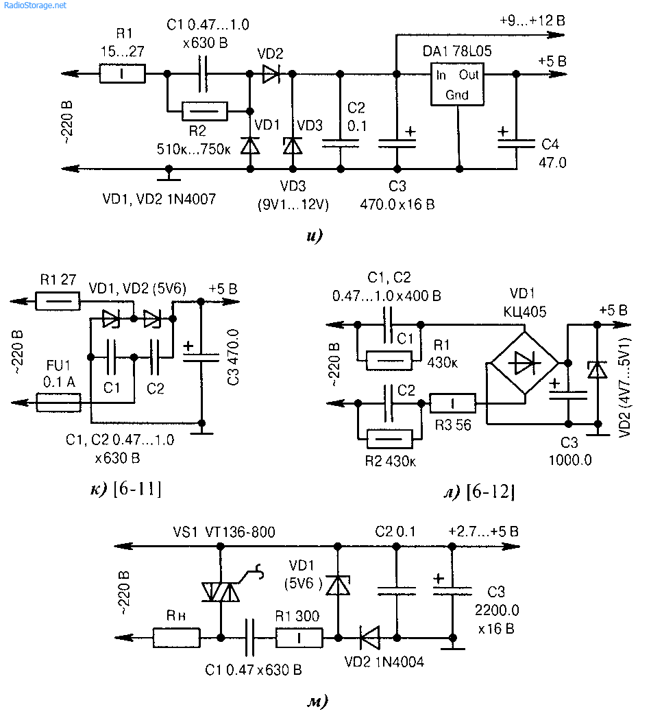
i) receiving two voltages from one power source. The total load current consists of the sum of the currents in the channels +9...+12 V and +5 V. If there are significant fluctuations in the load current, you should choose a VD3 zener diode with increased power dissipation of 1...3 W;
j) Zener diodes VDI, VD2 simultaneously serve as stabilizers and rectifiers. Zener diodes should be chosen that are powerful, with a current reserve;
l) instead of one, two ballast capacitors C1, C2 are used, which can be designed for a lower permissible voltage;
l) in the closed state of thyristor VS1, the current to the transformerless voltage stabilizer (C1...CJ, RL..R3, VDI, VD2) passes through the load RH. Due to the low current value, the load does not operate at full capacity, for example, the lamp does not light, the fan does not spin, etc. After turning on the VSI thyristor, full power is supplied to the RH load, and the voltage at the stabilizer output decreases from +5 to +2.7 V. For the MK to function normally, it must have a wide-range power supply and be able to organize a restart.
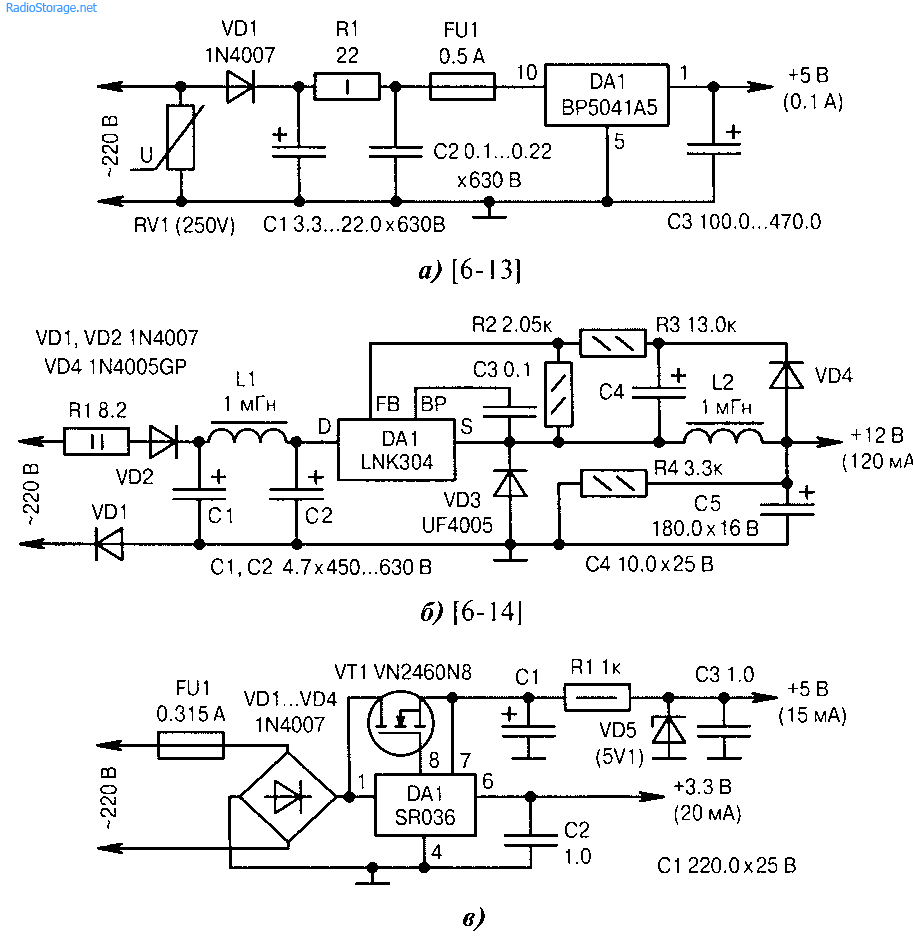
Rice. 6.4. Schemes of network transformerless power supply units with AC/DC converters:
a) a typical circuit for connecting a pulsed AC/DC voltage converter on a DA1 microcircuit from ROHM;
b) a typical circuit for connecting a pulse AC/DC voltage converter on the DA1 microcircuit from Power Integrations. Chokes LI, L2 reduce the level of pulsation;
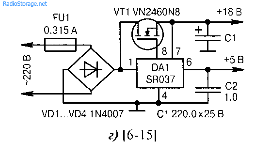
c) a driver for two supply voltages popular among radio amateurs: +5 and +3.3 V. The DA1 microcircuit is a pulse AC1DC voltage converter from Supertex;
t) DAI is a pulse AC1DC voltage converter from Supertex. The total load current across the +18 and +5 V outputs should not exceed 40 mA.